Continue to Site

Welcome to EDAboard.com

Welcome to our site! EDAboard.com is an international Electronics Discussion Forum focused on EDA software, circuits, schematics, books, theory, papers, asic, pld, 8051, DSP, Network, RF, Analog Design, PCB, Service Manuals... and a whole lot more! To participate you need to register. Registration is free. Click here to register now.

Simulation of opamps in Cadence

theguardian2001

Newbie level 5
Newbie level 5
Joined
Sep 29, 2024
Messages
10
Helped
0
Reputation
0
Reaction score
0
Trophy points
1
Activity points
142
Hi, everyone! I have recently posted a thread about getting error in dc simulation for a folded cascode opamp. Please see it for a full explanation: https://www.edaboard.com/threads/er...gence-in-cadence-spectre.412563/#post-1781856
To keep things shorter: Cadence did not want to converge because it had not seen any resistance between drain and source of a couple of cascoded PMOSes. I tried several things to overcome the problem. The latest was simply inserting one more PMOS pair inbetween the original ones and the output terminal such that Spectre "skips" or "leaves shorted" the ones with zero rds - have not helped.
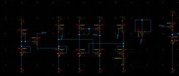
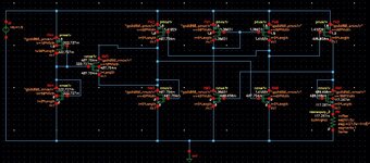
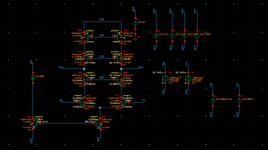
After a while I swithced the technology to free PDK45 thinking that the error was in the technology files. However, today I tried to test the new technology with the telescopic opamp. The results have almost freaked me out: for this technology by testing the op in the dc analysis all of the voltage headroom is now occupied by exactly these two PMOSes which have not consumed any voltage at all in the previous simulations (these are named in schematic as PM1 and PM2). So I am thinking that there is something wrong with the setup/simulator because the error appers for exactly the same devices. I am attaching schematic, testbench and log file. I would really appreciate any comment and advice regarding the issue.
P.S. Probably my explanation of the issue was not the best. However, in the context of the previous thread it makes much more sense.
 

Attachments

  • log_telescopic.txt
    10.5 KB · Views: 11
  • netlist_telescopic.txt
    94.9 KB · Views: 17
  • telescopic_1.png
    telescopic_1.png
    23.7 KB · Views: 29
Again, these are fake (non-silicon, just how "real" when there's nothing to "fit"?) devices / models, right? I advised a closer look at FET I-Vs to see if the problem is "from above".

A thing to look at, is whether the S, D diodes have any model properties populated, and whether individual devices have junction area and periphery props set, to scale them for C and (you wish) leakage. Also, a realistic FET will have channel leakage from the surface states (NFS in older models, dunno what yours look like). If your sub threshold slope looks "too good to be true" then maybe it is.
 
  • There is no proper connection in current mirror
  • Transistors are biased by voltage
  • The circuit is suppose to be a high gain OTA, while no feedback is present.
All above means it is not working and it is normal behavior.
 
Again, these are fake (non-silicon, just how "real" when there's nothing to "fit"?) devices / models, right? I advised a closer look at FET I-Vs to see if the problem is "from above".

A thing to look at, is whether the S, D diodes have any model properties populated, and whether individual devices have junction area and periphery props set, to scale them for C and (you wish) leakage. Also, a realistic FET will have channel leakage from the surface states (NFS in older models, dunno what yours look like). If your sub threshold slope looks "too good to be true" then maybe it is.
Good afternoon, dick_freebird! I really appreciate both of your responses. To be honest, I am not entirely sure what do you mean by the sentence: "A thing to look at, is whether the S, D diodes have any model properties populated, and whether individual devices have junction area and periphery props set, to scale them for C and (you wish) leakage." Can you please explain in little bit more detail what do you mean by that? As you mentioned, the I-V characteristics are the first thing I haven taken a look at even before testing this very circuit. (To be honest these ones I tested for gpdk090 and not for this one). They look a the one I would expect yo see from a short-channel devices.
--- Updated ---

  • There is no proper connection in current mirror
  • Transistors are biased by voltage
  • The circuit is suppose to be a high gain OTA, while no feedback is present.
All above means it is not working and it is normal behavior.
Thank you, Dominik, for your response! You are absolutely right regarding the CM connection - I was just stacking on transistors for this technology to see if Spectre gives any reasonable dc op for the analysis. That might actually be a problem which is sometimes really hard to detect when one focuses on the cascode but not the basics. However, I can not really agree on two other notices regarding the circuit. Yes, transistors are biased by voltage rather then a current. The reason comes from the previous thread. The voltages I have peaked up has been generated through a successfully-tested beta-ratio multiplier for gpdk090. The sizing for the other technology, as well as bias voltages and supply stays the same. I do not want to say that I would expect 45nm tech behave the same as 90nm even with the same sizing - just to troubleshoot the error in spectre or model files by switching to the other technology. Regarding the third bullet point I would rather partially agree then disagree. The reason for that is that I would like to see the open loop gain of the opamp first before putting in in a feedback configurations. Even though open-loop gain is tested by stb analysis for a fully-differential configuration, which is the case for me, the first thing to do before starting on checking the specs is a simple dc op, which, again, I have been trying to do here. I would like to see some reasonable overdrive across all the devices in cascode and the output slopes to get a zero-order's estimation for the gain. Or have you meant the common-mode feedback?
Anyways, thank you so much for help!
 
Last edited:
My thinking is that a circuit should still "solve" to "something" even if hooked up wrong. The convergence problem says maybe too little conductance somewhere, insane gain or polystable circuit operation (hysteretic, latching).

Maybe the issue-set is changing shape as we go. But gross convergence problems are bad news for design progress and maybe a manifestation of "GIGO".
 
Yes, transistors are biased by voltage rather then a current.
MOSFETs are biased by current through current mirror. This is the only way to bias any MOSFET properly. Even simplest CS amplifier has to be biased by current through current mirror, while signal is DC blocked. By voltage, you can bias BJT not MOSFET.
The reason for that is that I would like to see the open loop gain of the opamp first before putting in in a feedback configurations.
It is not possible to get OL gain with no feedback configuration as OTA cannot be biased in proper operating point.
the first thing to do before starting on checking the specs is a simple dc op, which, again, I have been trying to do here. I would like to see some reasonable overdrive across all the devices in cascode and the output slopes to get a zero-order's estimation for the gain.
Again, with no feedback (both differential and CMFB) you cannot expect any results. The input range of differential pair is around 50mV (depending to it OP). With 80dB OL Gain you have to set differential voltage between inputs with 1µV accuracy only because of gain. Any difference will strongly affect current in both OTA branches results in different OP of OTA transistors. You can play like this for long time getting nothing valuable.

Do things in proper way. You are getting errors in simulations not because something is wrong with gpdk (both gpdk090 and 45 are mature and well tested even if they are not real process) or simulator, but because testbench is wrong.

Start from single ended version in unity gain configuration. Then expand it to fully differential.
 
MOSFETs are biased by current through current mirror. This is the only way to bias any MOSFET properly. Even simplest CS amplifier has to be biased by current through current mirror, while signal is DC blocked. By voltage, you can bias BJT not MOSFET.

It is not possible to get OL gain with no feedback configuration as OTA cannot be biased in proper operating point.

Again, with no feedback (both differential and CMFB) you cannot expect any results. The input range of differential pair is around 50mV (depending to it OP). With 80dB OL Gain you have to set differential voltage between inputs with 1µV accuracy only because of gain. Any difference will strongly affect current in both OTA branches results in different OP of OTA transistors. You can play like this for long time getting nothing valuable.

Do things in proper way. You are getting errors in simulations not because something is wrong with gpdk (both gpdk090 and 45 are mature and well tested even if they are not real process) or simulator, but because testbench is wrong.

Start from single ended version in unity gain configuration. Then expand it to fully differential.
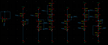
That makes sense. I am completely agree that transistors should be biased with a curret rather then a voltage. However, I am not really sure if that makes a difference for the simulator. Please correct me if I am wrong: When a current is passing through a diode-connected device, it generates the gate-source voltage needed for this device to maintain the same current; thereafter this gate-source voltage can be applied to the gate of the other device one can expect the second transistor to reproduce the mentionedd current. The voltages I am applying to the gates were previously generated by this circuit, which has been successfully tested.
IMG_0078.jpeg

I tried to remove this circuit from the cellview and expected that it might be easier for cadence to converge the solution.
So, my question can be rather formulated like the following: Does it make the difference in that very case if one inserts the full bias circuit to the opamp's schematic or if one just inserts the dc sources with dc voltage equal to the corresponding ones from the bias circuitry?
Anyway, I will actually start the verification with the steps that you have mentioned. Thank You a lot, Dominik!
 
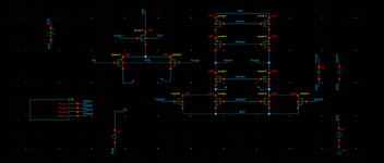
Hello, everybody! I have tried to start the simulation by connecting the opamp in unity-follower configuration with the single-ended output and using the biasing circuitry instead of constant dc sources. I tried to do it with gpdk090 since I had a biasing circuitry for this technology sucsesfully tested from before. However, Spectre faces even more convergence problems with such a setup compared to the version with constant sources. I am not really sure what I am doing wrong in that case :(

Based on the log file I would guess that the problem spectre is facing is instability to find a suited operating point. At the same time one knows that a follower configuration is the worst one for stability and one may not use the opamp as a buffer. So I would pretend to say that having an unstable opamp in a buffer-connection does not automatically mean that it can not be used with some other feedback (f. e. resistive), isn't it?
 

Attachments

  • Biasing_1.png
    Biasing_1.png
    17.6 KB · Views: 13
  • Biasing_2.png
    Biasing_2.png
    21.1 KB · Views: 12
  • Folded_follower.png
    Folded_follower.png
    17 KB · Views: 11
  • log_folded_follower.txt
    22.7 KB · Views: 8
  • Netlist folded follower.txt
    96.8 KB · Views: 8
Attached netlist is incomplete.
You are using global nets in subcircuit but not on the top level, so there is no supply connection in the instance I10. At least according to attached screenshots.

Something is fishy also, as in log spectre is complaining on lack of dc path between net Vip and 0. Looks like some nets are floating for some reason. It might results with some strange conditions for model, what could end up with shorts.
  1. Make supply nets global
  2. add nodeset for your biasing circuit (startup circuit is working in transient, not in dc)
  3. and please attach full netlist
Good afternoon, Dominik and thank you for your reply! Yes, the supply connections have been messed up. I changed all of them to global ones which can be seen from the netlist. This time I extracted the whole one 😅

I have also added a nodeset and removed the start up circuitry from the bias cell. I have checked with one of my previous simulations of the bias circuitry before and set nodes according to the derived op. However, after these manipulations the output log file looks exactly the same with the only exeption for an instance name of a bias cell since it has been modified. I am completely agree with you regarding the lack of dc path even though "Check and save" has not shown any missing connections/floating nodes. Plese see the full netlist and updated log file in the attachements.

As always, I would be happy to hear anny suggestions.
Thamk you in advance.
 

Attachments

  • input.txt
    104.8 KB · Views: 3
  • spectre.txt
    23.8 KB · Views: 2
  • IMG_0079.jpeg
    IMG_0079.jpeg
    145.7 KB · Views: 4

LaTeX Commands Quick-Menu:

Part and Inventory Search

Welcome to EDABoard.com

Sponsor

Back
Top