Continue to Site

Welcome to EDAboard.com

Welcome to our site! EDAboard.com is an international Electronics Discussion Forum focused on EDA software, circuits, schematics, books, theory, papers, asic, pld, 8051, DSP, Network, RF, Analog Design, PCB, Service Manuals... and a whole lot more! To participate you need to register. Registration is free. Click here to register now.

Simulation Momemtum ADS

Status
Not open for further replies.

ads_begginer

Newbie level 5
Newbie level 5
Joined
Mar 21, 2019
Messages
8
Helped
0
Reputation
0
Reaction score
1
Trophy points
1
Activity points
75
Hello everyone

My goal is to make a amplifier lna
I want to do a momemtum simulation of a design on ads and then simulate with a schematic.

first I simulated the S parameters of my amplifier and I get the following performances(picture 1).

Then I made the layout of my amplifier with CPWG lines.
To perform the momemtum simulation I configured the substrate as well as the ports (picture 2) following the ads tutorial:


https://literature.cdn.keysight.com/litweb/pdf/5992-1632EN.pdf?id=2758796


Once the momemtum simulation is finished, I create a model and a symbol and then I import it into my schematic to simulate the S parameters.
So my problem is this: I get horrible performances that are completely different from what I should get. (picture 3).

What is the reason for this horrible performance?

In addition during the simulation momemtum warnings appear but I do not understand the messages(picture 4).


Can someone please help me to get the correct performance?

kind regards
 

Attachments

  • picture 1.pdf
    347.8 KB · Views: 141
  • picture 2.pdf
    236.4 KB · Views: 133
  • picture 3.pdf
    220.6 KB · Views: 127
  • picture 4.pdf
    192.5 KB · Views: 128

Please show a detail view where exactly you placed the ground pins.

There is a typical mistake for CPW that happens when you ground place pins on a wide edge: ADS creates ports that are wide compared to the wavelength. But for valid results, port width must be small w.r.t. wavelength

cpw.PNG

Solution: specify an explicit width for the ground pins, as I described in my appnote:
https://muehlhaus.com/support/ads-application-notes/edge-area-pins
 

Hello thank you for your interest in my problem.

actually my ground pins were placed a little bit randomly.

So I read your document about edges/area pin and used edge ports for my ground pins (picture 1) but the pin for the cpw line is defined as a dot (P1 on my picture).

so I have a few questions.

first of all when I created my rectangle for the ground, I chose a random height. does this have any impact?
then I created my edges pins for the ground. but does the length of the line have any impact? if yes how to define it?

thank you in advance

kind regards
 

Attachments

  • picture1.PNG
    picture1.PNG
    28.3 KB · Views: 126

Hello thank you for your interest in my problem.
actually my ground pins were placed a little bit randomly.
So I read your document about edges/area pin and used edge ports for my ground pins (picture 1) but the pin for the cpw line is defined as a dot (P1 on my picture).
so I have a few questions.
first of all when I created my rectangle for the ground, I chose a random height. does this have any impact?
then I created my edges pins for the ground. but does the length of the line have any impact? if yes how to define it?
thank you in advance
kind regards

This is not an appropriate Port configuration.Calibration will fail..
 

Indeed, it generates other warnings messages.
for example : The size of the minus pin for S-parameter port 1 is electrically large above 3.20013 GHz, S-parameters may become unphysical.

so I looked at this application note to understand my mistakes: https://literature.cdn.keysight.com/litweb/pdf/5992-0415EN.pdf

I want to simulate my design from 2 to 26 Ghz. so the distance between my pin 1(P1) and my ground pins(P5 and P6) must be smaller than 10% of the wavelength at the highest simulation
frequency.

Does this seem like a good approach to solving my problem?

thank you.
 

I corrected the warnings messages by bringing the ground pins pin closer to the transmission line but when I simulate with the schematic my performance remains mediocre.

Somebody can help me, please.
 

I corrected the warnings messages by bringing the ground pins pin closer to the transmission line but when I simulate with the schematic my performance remains mediocre.
Somebody can help me, please.

How is the equivalent schematic of this layout ? I cannot see any equivalency in regard of it..
 

How is the equivalent schematic of this layout ? I cannot see any equivalency in regard of it..

please find attached my schematic as well as my layout and the co simulation with the performances.

the frequency that interests me is at 24 ghz.
 

Attachments

  • schematic_line_CPWG.PNG
    schematic_line_CPWG.PNG
    24 KB · Views: 172
  • perf_schematic_line_CPWG.PNG
    perf_schematic_line_CPWG.PNG
    43.2 KB · Views: 118
  • layout_line_CPWG.PNG
    layout_line_CPWG.PNG
    43.8 KB · Views: 135
  • configurations_pins.PNG
    configurations_pins.PNG
    18.7 KB · Views: 164
  • schematic_cosimulation.PNG
    schematic_cosimulation.PNG
    13.2 KB · Views: 155
  • perf_cosimulation.PNG
    perf_cosimulation.PNG
    48.3 KB · Views: 129

-The schematic is not equivalent of the layout at all.. Once, the layout is asymmetric so the circuit CPWG model cannot represent the layout..You layout has no equivalent schematic .
-You ignore T-Junction between CPW Transmission Lines, it's an error..

Are you trying to match an active device ?? If it's so, why you use CPW ?? What is your purpose ??
 

Okay, if I understood correctly I can't simulate my layout from the schematic. In this case how can I check if my layout corresponds to my expectations?

Otherwise I ignored the T-junction because on ads they do not exist with cpw lines.

what I'm trying to do is to make an lna amplifier. the left part of my layout represents the input adaptation, the right part represents the output adaptation and in the middle there's my box with the S parameters of my transistor.
I use cpwg lines because at high frequencies it's these types of lines that are favoured
 

So I read your document about edges/area pin and used edge ports for my ground pins (picture 1)

It seems that my appnote confused you, your new configuration is completely wrong. The line for the ground pin must be small and near the gap -- not on the complete edge!

The pin configuration in your post #8 is correct.

~~~

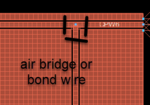
One problem with your CPW design is that your layout has no air bridges between the ground areas. The schematic model assumes good connection of all ground areas.

bond.PNG
 
Last edited:
do you have any documents regarding the bond wire design, please?
 

Status
Not open for further replies.

Part and Inventory Search

Welcome to EDABoard.com

Sponsor

Back
Top