Continue to Site

Welcome to EDAboard.com

Welcome to our site! EDAboard.com is an international Electronics Discussion Forum focused on EDA software, circuits, schematics, books, theory, papers, asic, pld, 8051, DSP, Network, RF, Analog Design, PCB, Service Manuals... and a whole lot more! To participate you need to register. Registration is free. Click here to register now.

Simulate linearity parameters of a fully differential OTA

Status
Not open for further replies.

shimaa.heydari

Junior Member level 1
Joined
Oct 21, 2017
Messages
16
Helped
0
Reputation
0
Reaction score
0
Trophy points
1
Activity points
158
hello all friends
i want to simulate linearity parameters such as THD, IM3, IP3 of an OTA with two output node (in other word this is fully differential).
my problem is in the output nodes.

1- I have two node in output. what I insert to this nodes?(R or C) with how much value?
2- what is correct to simulate? the linearity of voltage or current? in other word I must simulate THD of current or voltage?
 

It depends on impedance of next stage.
Here you have to consider modes, differential and common.
 

It depends on impedance of next stage.
Here you have to consider modes, differential and common.

There is no next stage. only one OTA.

in some papers the authors report The THD of Only theirs proposed OTA. then use this transconductor in a filter. but I have no filter.

i want to khow for example when they tell us THD of OTA is -40dB or THD of filter is -50 dB, exactly they point to where of circuit?
what means the the THD of OTA?
I see in an article that author first put a 1 Ohm resistor between two output nodes of OTA.
then measured the THD of Current Passing in this small resistor. is this method valid?
 

You should be aware that a real amplifier is driving a load, otherwise it would be useless.

Specifying the load for your OTA simulation is a matter of convention respectively the intended application. Using a low load impedance value like 1 ohm is a valid choice to have little influence of OTA output impedance on the measurement. But there are other possible choices.

i want use OTA for Gm-C filters. I want to measure Linearity parameters of my proposed OTa. what is the conventional method that used in valid articles?
what are they doing in output nodes of OTA when they report parameters of their proposed OTA in a table?
 

what is the other possible choices?
please guide me or give me a valid reference.
 

HTML:
OTA is no more than voltage amplifier which output impedance is high.

Simply apply load which is used in your application.

Can you understand very basic things surely ?

There is no next stage. only one OTA.
Simply you can not understand very basic things at all.

Loads must exist in any circuit.
Open drain can not exist.
 

I am sorry. I can not tell you my really purpose...:sad: :bang:

I know each amplifier must drive a load. ok. this is clear.

my question is how to test an OTA. papers don't tell what is the properties of they load for testing linearity of OTA. they just report linearity values in their tables.
for example IP3 is 20dB. good! but they don't say:

1- IP3 of output voltage or current?
2- with what kind of load?
3- how connected this load?

only in one paper i read: author measured the im3 of current passing through an 1 Ohm resistor that connected between two output nodes of OTA.
 

As previously mentioned, effective output short (low resistor value or current probe) connected between differential output terminals is a valid choice. It can be expected to access the dominant non-linearity effect located in the input stage. Voltage dependent output impedance may add non-linearity in a gm-C application, you also want to determine the useful voltage swing which can be only determined with non-zero load impedance.

Appropriate common mode bias is presumed in any case.
 

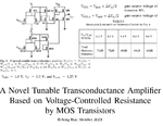
this is my paper that i want to simulate.
"A Novel Tunable Transconductanse Amplifier Based on Voltage-Controlled Resistance by MOS Transistors-2006"
first I put a 1 Ohm resistor between output node to Ground. THD= -29dB obtained!
this is wrong. in table 1 of this pepar THD=-70 dB for (Vp-p=0.2 and Vindc=1.25) input voltage.
second I put a 1Pf capacitance. then THD= -60dB for current and -66.6dB for voltage Obtained.
but I want -70 dB!
input Gate voltage are(1.25±0.2/2) as determined in article.
I use thd_func() in ADS and HB simulator.
what is wrong? please :sad:
 

Attachments

  • Untitleed.png
    Untitleed.png
    11.9 KB · Views: 110
  • +TCSII.2006.875309_e6eeb94b048de1305ca17b8bf9e4e2d1.pdf
    458.6 KB · Views: 93
  • Untitledd.png
    Untitledd.png
    107.2 KB · Views: 123
Last edited:

first I put a 1 Ohm resistor between output node to Ground.
THD= -29dB obtained!
this is wrong.
This is very natural result.
Do you think this can keep appropriate bias points ?

Evaluate OTA as either of followings.
(1) Evaluate output voltage with no load.

(2) Evaluate output current as resistor. Here connect outputs to inputs.
In this casem input current is equal to output current.
 

first I put a 1 Ohm resistor between output node to Ground
No idea what this means. You have 2 output nodes, ground node and one resistor, what's the circuit?
 

to FvM:
this is a test circuit.
i upload pictures and the pdf of article in this post...
my OTA has two output node. but in this article OTA has one output(single ended). i want to simulate this paper to evaluate the structure of out put. if i can obtain THD=-70, as mentioned in table 1 of paper, then I can learn What i do in my fully differential OTA. this is an example.
but Unfortunately i failed to obtain -70 that is correct.
please help me...

- - - Updated - - -

to pancho_hideboo:

(1) i evaluate output voltage with no load: THD=-21.77 obtained. that is not desired because THD=-70.

(2) I can not understand what you mean? I want THD=-70 as mentioned in table 1 of this paper. only this! may i request you see the paper? i upload that.
 

(2) I can not understand what you mean?
Can you understand basic building block in gm-C filter ?
Resistor connection is a one of them.

However Your DUT is :
Differential Inputs.
Single-Ended Output ?

This is contradictory with title of this thread, "Simulate linearity parameters of a fully differential OTA".

First do DC analysis with delta_Vin=0.0 and no load.
Then evaluate operation point voltage of out node.
This is an equilibrium operation point.

Next connect DC source of this voltage value to out node as load.
This is a very ideal load for OTA.
Then do HB analysis with not zero delta_Vin.

Guessing from your previous post, https://www.edaboard.com/showthread.php?t=372232
you can not understand very basic things at all.

Show us Simulation Netlist and Schematics where operation points informations are annotated.
 
Last edited:
  • Like
Reactions: FvM

    FvM

    Points: 2
    Helpful Answer Positive Rating
you have right pancho_hideboo...
first I must thank to you for your good help with pictures for plotting Gm in ADS.
My question was contradictory with title of this thread, "Simulate linearity parameters of a fully differential OTA". ok.
but i said this to "we having a really example with knowing the value of THD=-70dB".
after this we discuss about fully differential OTA. well?

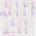
i upload the schematic (with DC analyze) of that papers circuit.

first i zero the Δvin=0. operation point at out node obtaines 1.13 as bold in picture1.
second i put a DC supply=1.13v at out nod. now i insert a current prob with DC Supply and put Δvin=0.2 as picture 2.
thired I do HB simulation with Δvin=0.2 as third picture.

1- THD=-64.544 for current of DC supply obtained that is not -70 dB again. every thing is in 0.18um technology same in the paper.
2- THD of vo errored! because this is ideal DC supply??

what is wrong? simply and step by step please.
 

Attachments

  • paper1.png
    paper1.png
    88.2 KB · Views: 102
  • paper12.png
    paper12.png
    47.9 KB · Views: 109
  • papar13.png
    papar13.png
    66.2 KB · Views: 102

Did the authors of the paper obtain this THD in ADS environment or Cadence ADE ??
 

Did the authors of the paper obtain this THD in ADS environment or Cadence ADE ??

hello BigBoss
None of them. they worked in HSPICE 0.18 µm standard CMOS Technology.

is it important?
i uploaded this paper in this thread. can you see?
 
Last edited:

-64 versus -70 dB isn't so much different. My guess is that the nonlinearity is located in diff pair and characteristic for the given transistor parameters and operation point. You can check the assumption by locking at different circuit currents and voltages.
 

hello BigBoss
None of them. they worked in HSPICE 0.18 µm standard CMOS Technology.

is it important?
i uploaded this paper in this thread. can you see?

It might be important because ADS or Cadence Spectre may differently interpret-mostly- the model parameters of a technology.And this may bring a comparable difference.
That's why I'm asking which simulator has been used.Another 3rd part simulator-for instance ELDORF or Nexxim- also will interpret the model or model metrics quite different.
This is important..
For example..
While I'm obtaining -25dBm 3rd Harmonic Power Level of an oscillator in ADS, Cadence Spectre gives me-for the exactly same circuit- -32dBm.
This is included in THD computation.6dB difference may come from a such interpretation.If the paper is not IEEE ask the mods. to post it here.There are some constraints about papers here.
 

Status
Not open for further replies.

Part and Inventory Search

Welcome to EDABoard.com

Sponsor

Back
Top