Continue to Site

Welcome to EDAboard.com

Welcome to our site! EDAboard.com is an international Electronics Discussion Forum focused on EDA software, circuits, schematics, books, theory, papers, asic, pld, 8051, DSP, Network, RF, Analog Design, PCB, Service Manuals... and a whole lot more! To participate you need to register. Registration is free. Click here to register now.

Simple question regarding an amplifier

Status
Not open for further replies.

stamford

Newbie level 6
Newbie level 6
Joined
Sep 20, 2009
Messages
13
Helped
1
Reputation
2
Reaction score
1
Trophy points
1,283
Location
usa
Activity points
1,385
Hi all,
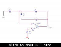
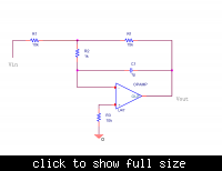
I came across a simple inverting amplifier circuit. It has a capacitor in parallel to the feedback amplifier.
I can tell the circuit functions as an inverting amplifer with a gain of 15 and that no (negligible ??) current flows through the capacitor and the 1k resistor.
Can anyone please tell me whats the function of the 1pF capacitor and the 1K resistor ? .
 

I wish you had looked better into the circuit before replying. It clearly isn't an integrator. Its an amplifier. An integrator has a capacitor, alone in the feedback. Not a resistor in parallel with it.
 

Can anyone please tell me whats the function of the 1pF capacitor and the 1K resistor ?

It is new to me too though I worked a lot with opamps. So I am curious as you are to know how the 1pF and 1K can affect one or more features of the new amplifier. But first, it is better to specify the type of the opamp supposed to work better after adding these two components.

Kerim
 

At "low" frequency the op amp Rf = 15K, when the signal frequency start rising at frequency equal to
Fp = 1/( 2 * pi * ( RF + R2) * C1 ) the voltage gain start to drop and at frequency Fz = 1/ ( 2 * Pi * R2 * C1) the gain stop to the decrease.
And the new gain is set and equal to
Av = (RF||R2)/R1
 

The opamp is OPA131 from TI. However, I can't find anything in the literature to suggest the use of these two components

---------- Post added at 17:42 ---------- Previous post was at 17:34 ----------

---------- Post added at 17:45 ---------- Previous post was at 17:42 ----------

At "low" frequency the op amp Rf = 15K, when the signal frequency start rising at frequency equal to
Fp = 1/( 2 * pi * ( RF + R2) * C1 ) the voltage gain start to drop and at frequency Fz = 1/ ( 2 * Pi * R2 * C1) the gain stop to the decrease.
And the new gain is set and equal to
Av = (RF||R2)/R1

It looks correct mathematically. Could you also elaborate what's the advantage/disadvantage of having this sort of feature. I haven't seen this kind of arrangement used at all
 

It looks correct mathematically. Could you also elaborate what's the advantage/disadvantage of having this sort of feature. I haven't seen this kind of arrangement used at all
No, my previous post is wrong. I overlook the diagram and described this circuit.

Sorry for the error
 

Hi all,
I came across a simple inverting amplifier circuit. It has a capacitor in parallel to the feedback amplifier.
I can tell the circuit functions as an inverting amplifer with a gain of 15 and that no (negligible ??) current flows through the capacitor and the 1k resistor.
Can anyone please tell me whats the function of the 1pF capacitor and the 1K resistor ? .


I think that it is a way how to do frequency compensation of this amplifier in order to provide its stable behavior.
Try the following:
1) Make the wye-delta transformation of R1, Rf, and R2. You obtain resistors Ra, Rb, Rc; Ra=11.666kOhms between Vin and - nodes, Rb=17.5kOhms between - and Vout nodes, and Rc=165kOhms between Vin and Vout terminals.
2) Rc does not affect the amplifier behavior since it is between Vin and Vout, thus it is not necessary to consider it.
3) R3 is only for current offset compensation. It does not affect the amplifier gain.
4) Considering 1) to 3), your circuit can be simplified to OmpAmp with Rb in parallel to C1 in the feedback path, and Ra in the forward path. Then the DC gain is equal to -Rb/Ra=-1.5.
5) The schematic 4) with small capacitor C1 represents the so-called "lead compensation". The product Rb*C1 forms the transfer zero in the circuit transfer function on the frequency 1/(2*pi*Rb*C1)=9MHz. It serves for the compensation of the OpAmp second pole which is anticipated on this frequency. In addition, C1 adds also one pole to the transfer function at the frequency 1/(2*pi*Rb//Ra*C1)=22.7MHz. However, it is far from the second pole, thus it does not cause problems in terms of the circuit stability.
For more details, see, for example, the file
**broken link removed**
pages 9-10.
 
OK I done some math once more, and this is what I get.

The gain at low frequency is equal to

Av = RF/R1 = 1.5 V/V

But at frequency equal to

\[ Fo = \frac{R1}{ 2 *\pi * C1 (R1*R2 + R1*RF + R2*RF) } = 9MHz\]

At this point the voltage gain start to drop 20dB per decade.

Of course in real life the gain will start drop much faster.
For OPA131 the gain will drop close to 250KHz.
So it seems that this additional RC circuit improves stability of the circuit.
 
Last edited:
OK I done some math once more, and this is what I get.

The gain at low frequency is equal to

Av = RF/R1 = 15 V/V

But at frequency equal to

\[ Fo = \frac{R1 - 2}{ 2 *\pi * C1 (R1*R2 + R1*RF + R2*RF) } = 5.1MHz\]

At this point the voltage gain start to drop 20dB per decade.

Of course in real life the gain will start drop much faster.
For OPA131 the gain will drop close to 250KHz.
So it seems that this additional RC circuit improves stability of the circuit.

Yes, but there are two points which should be cleared up:
1) The gain is Av=-RF/R1=-1.5
2) \[ Fo = \frac{R1}{ 2 *\pi * C1 (R1*R2 + R1*RF + R2*RF) } = 9MHz\]

The formula can be simplified to
\[ Fo = \frac{1}{ 2 *\pi * C1 (R2 + RF + R2*RF/R1) } = 9MHz\]

The "resistive" term is Rb (the well-known formula for wye-delta transformation). Then you obtain my result above.
D.
 
Yes you right, I use R1 = 1K so this is why "my gain" is equal to 15V/V (and Fo=5.1Mhz) instead of 1.5V/V
And to find Fo i use "brute force" (nodal analysis).


For node A

\[\frac{Vin - Va}{R1} = \frac{Va-Vb}{R2}+\frac{Va-Vout}{Rf} \]

And for node B

\[\frac{Va-Vb}{R2} = \frac{Vb-Vout}{\frac{1}{s*C1}} \]

And the voltage gain

\[Av(s) = -\frac{Rf}{ R1 + C1*(R1* R2 + R1*RF + R2* RF)*s } \]


But your method is much more simpler I never thought about wye-delta transformation, nice trick.

I corrected all the errors I made.
 
Last edited:
OK, it is clear now..:-D
D.
 
Thank YOu Dalibor and Johny130. That was great analysis, It did really clear up my confusion.
 
Status
Not open for further replies.

Similar threads

Part and Inventory Search

Welcome to EDABoard.com

Sponsor

Back
Top