Continue to Site

Welcome to EDAboard.com

Welcome to our site! EDAboard.com is an international Electronics Discussion Forum focused on EDA software, circuits, schematics, books, theory, papers, asic, pld, 8051, DSP, Network, RF, Analog Design, PCB, Service Manuals... and a whole lot more! To participate you need to register. Registration is free. Click here to register now.

Simple CMOS Analog Square-Rooting and Squaring Circuits

Status
Not open for further replies.
Hi,

I opened the document, but didn´t go deeper in the formula.. So I can´t give an answer.

More than 20 years ago I had to design an analog multiplier circuit .. with ready to buy device. I was not allowed to do this digitally.
But in the very most cases I´d perfer the digital processing, because they are more precise and more flexible.

May I ask why you want to do it with an analog circuit?
To be honest I find it a bit outdated. But don´t get me wrong, I like analog signal processing, but mainly just to feed ADCs with most perfect input signals.
And yes, I know, analog circuits have their benefits against digital circuits...in some details..

Klaus
 

Re: Simple CMOS Analog Square-Rooting and Squaring Circuits

how to derive equations 13 and 16 ?

From Equation 2 on it looks as though a lot of effort goes toward cancelling the effects of threshold voltages and mismatches between the nested transistors. Equation 1 depicts how voltage and current are related by the square root of 2. It becomes the basis for his circuit.

equation 1.png

Then although the article is "fundamental", the author seems to assume the reader has advanced knowledge. He puts formulae for k1 & k2 with no explanation about origin or meaning of terms:

formula k2 un Cox W L2.png

Equation 13 appears identical to #5. Equation 16 is almost the same. The premise is to operate the transistor close to pinch-off, near the limit of its operation. Response is non-linear, where small differences greatly affect results. Therefore most of the equations take k1 & k2 into account, for sake of accuracy. The reason is because real components have offset voltages and mismatches.
The op amp is a convenient method to solve these since the reference voltage is adjustable. The current source is adjustable. Gain is adjustable.
 
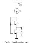
In Fig 1, Why would the lower transistor Q1 guaranteed to be in triode operating region ?

nested_transistor_pair.png
 

In Fig 1, Why would the lower transistor Q1 guaranteed to be in triode operating region ?

View attachment 158700

Although I'm not certain how to prove that...
I wouldn't be surprised if it has to do with this cause and effect below.

1) Voltage at the transistor gates causes both to conduct (as long as V is above a certain threshold level.)

2) Current through the lower transistor produces a voltage.

3) This voltage appears at the source terminal of the upper transistor, in effect changing its G-S relationship.

4) This alters its conductivity which affects current through it.

5) Current in the upper transistor is identical to that in the lower. The transistors influence one another by the above steps.

6) Equilibrium state is reached.

---------------------------------------

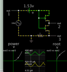
This simulation of the circuit illustrates. A picture is worth a thousand words.

A voltage sweep is applied instead of a fixed current source. This reveals behavior at very low current levels (near pinch-off region). Namely the exponential function of Amperes versus Volts.

mosfets voltage sweep (V-A plots power) (A-V plots root).png

Can we say the function definitely is square and square root? Or cube and cube root? Some effort might make it possible to bend response so it is mathematically accurate.
 

Why would the lower transistor Q1 guaranteed to be in triode operating region?
Counter question, do you understand why Q2 is in pinch-off? This should be your starting point.
 

Status
Not open for further replies.

Similar threads

Part and Inventory Search

Welcome to EDABoard.com

Sponsor

Back
Top