Jos Brink
Member level 3

Hello, can anyone help me with the following problem.
I've an ATmega128 connected to an external SRAM and an Ethernet MAC/ PHY. (ax88796b).
I want to use the address range 0x8000 -> 0xFFFF for the SRAM
and the range 0x4000 -> 0x7FFF for the ax88796 chip.
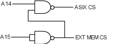
I came up with this simple address decoder (see attach) but i get weird timing problems. I can read/write to the SRAM with succes. But can't seem to write to the Ax88796 chip. All the chips are fast enough.
Can anyone verify if this circuit is suitable, íve seen designs where they combine the RD/WR signals to the decoder or CS lines. But what is the purpose of that?
Thank you all for your time.
Greetings from the rainy Netherlands.

