mtwieg
Advanced Member level 6

- Joined
- Jan 20, 2011
- Messages
- 3,916
- Helped
- 1,311
- Reputation
- 2,628
- Reaction score
- 1,441
- Trophy points
- 1,393
- Activity points
- 30,098
Another question from me about the UMC 65nm PDK...
I will need to create some 1.2V logic cells, but referenced to 1.2V (with a 2.4V supply) instead of the substrate. So I will need to use deep-N well/triple well nmos instead of normal nmos. The PDK has standard cells for these, which include the pwell and nwell surrounding regions. However to get good density I want the devices to share those wells so I can pack them with similar density to normal nmos. But they way the pdk works makes this difficult. As an example I have a simple two stage inverter layout.
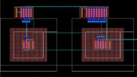
Here is each inverter spaced out so there's no overlap between the cells. The white hollow polygon is the nwell (NWEL). It has a void in the middle, for some reason. The inner reddish rectangle is the deep nwell (DNW).
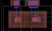
This is as close as I can get them before DRC errors kick in. The DNW are overlapping. DRC doesn't seem to mind that the NWEL from one cell is invading the empty void of the other cell's void in its NWEL...
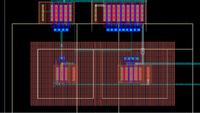
When I move them a bit closer, it complains about the NWEL from one cell being too close to the the features of the other. Quite strange, since I would assume that NWEL would be masked by DNW when generating the GDSII files.
The only way I can see to overcome this is to not use the standard dnw nmos layout cells, and make my own by using a standard nmos cells and surrounding them with my own NWEL and DNW. This passes DRC, and extraction seems to work all right as well, but LVS always fails.
Anyone have any idea how to get around this?
I will need to create some 1.2V logic cells, but referenced to 1.2V (with a 2.4V supply) instead of the substrate. So I will need to use deep-N well/triple well nmos instead of normal nmos. The PDK has standard cells for these, which include the pwell and nwell surrounding regions. However to get good density I want the devices to share those wells so I can pack them with similar density to normal nmos. But they way the pdk works makes this difficult. As an example I have a simple two stage inverter layout.
Here is each inverter spaced out so there's no overlap between the cells. The white hollow polygon is the nwell (NWEL). It has a void in the middle, for some reason. The inner reddish rectangle is the deep nwell (DNW).

This is as close as I can get them before DRC errors kick in. The DNW are overlapping. DRC doesn't seem to mind that the NWEL from one cell is invading the empty void of the other cell's void in its NWEL...

When I move them a bit closer, it complains about the NWEL from one cell being too close to the the features of the other. Quite strange, since I would assume that NWEL would be masked by DNW when generating the GDSII files.

The only way I can see to overcome this is to not use the standard dnw nmos layout cells, and make my own by using a standard nmos cells and surrounding them with my own NWEL and DNW. This passes DRC, and extraction seems to work all right as well, but LVS always fails.
Anyone have any idea how to get around this?

