Javert
Member level 2

Good day,
I am designing my first larger PCB with RF PA and a 100 pin processor.
Due to the lack of practical experience, I would like to bother with a few questions.
Board PCB is two side on FR4
1. RF
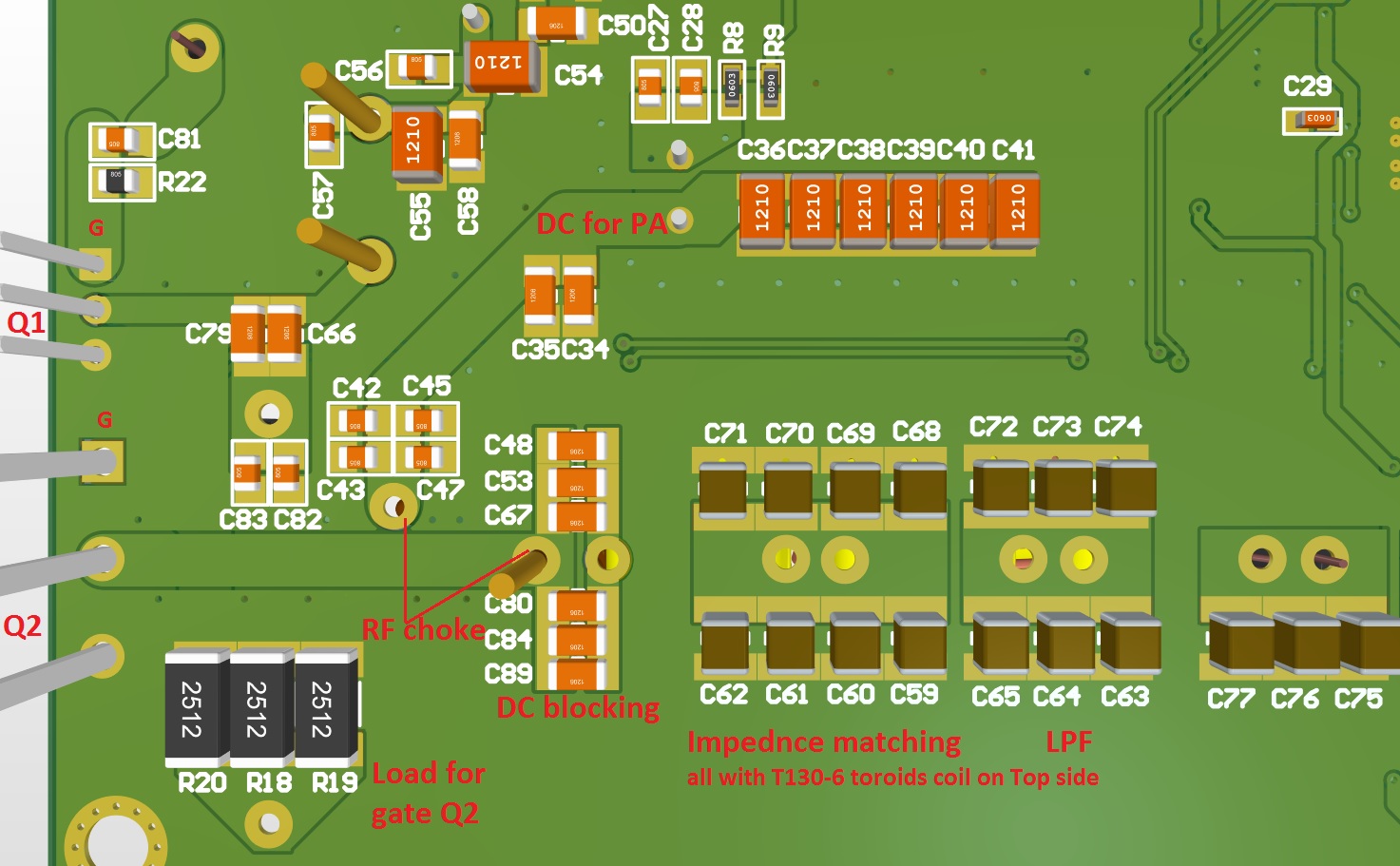
he RF part is two Mosfet trasnsistor PA in class C (100W 50V) 13.56MHz to 50ohm load.
On top side is toriods T50 - T130-6 SMD C and R on buttom side.
DC blockong C on class 200V
Brown Capacitor 1111 NPO 250V in impednce match and LPF
I have no specific question here
only when an experienced expert looks at it,
- do you see something downright bad, inappropriate?
- do you see something that could be improved, done differently?
2. PCB in general
Minimum Solder Mask Sliver (MSMS).
Altium altium has a rule MSMS.
Does it have any practical significance in conventional PCB design?
For example I have in design resistor networks 4x50ohm in size 1206 and her is real MSMS 0.047mm.
So should I set the rule to a minimum of 0.047 mm and not have more left, or does it have some practical meaning?
Silk To Solder Mask
For capacitors of size 1111, I have a frame around the component in overlay and it has a distance of only 0.035 mm from the solderm mask. Will it be a problem?
If so, what is the minimum distance you recommend?
Silk to Silk (Clearance=0.1mm)
what is the minimum clarence you recommend between silk?
What is the minimum font size?
For SMD I usually use 0.9mm, as a full minimum 0.8mm.
Won't it be too small for an ordinary Chinese manufacturer?
