Vermes
Advanced Member level 4

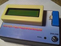
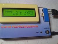
It is a design of semiconductor elements tester, inspired by the project from LINK. Original PCB was sawn to the housing (KM33A). Because 2x16 LCD displays with backlight are rather expensive, a removable module was made, which could be used in other devices. LCD joint was changed by moving the slot from the PCB to the housing.
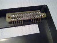
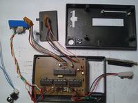
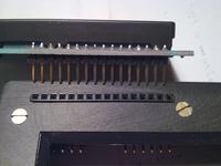
The device uses an external 9V power supply, at which when you insert the plug, you get a LCD backlight. At internal power supply it is turned off because of saving the battery. Meassuring sockets were removed from old TV sets. Blue solid ones have six inputs, what was used for the duplication and measures the elements in large housings. Sticked small white socket can be used for measuring such transistors as BD 137, BC 107.

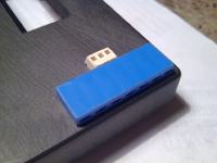
All three sockets are connected in parallel. Callibration button „KAL” and power switch are derived on the panel. Unnecessary „window” in the housing was sealed, over treated and sanded to a flat surface.
LCD backlight is taken from a separate stabilizer 7805 connected by a rectifying diode to plus of the power socket. Power switch is on minus cable.


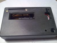

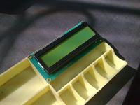
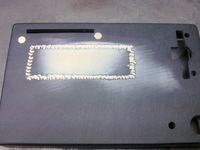
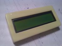
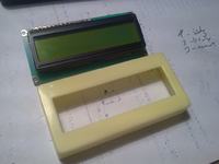
Self-adhesive rubber feet were glued from the bottom. Calibration can be made by short circuit of three inputs of the socket, holding down the momentary button „KAL” and turning on the power. Then follow the steps displayed on the LCD.


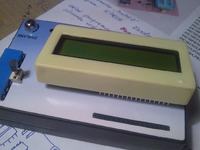
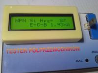
Tests:
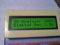

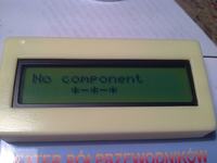
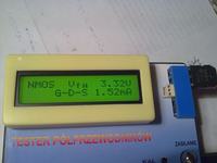
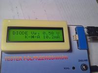
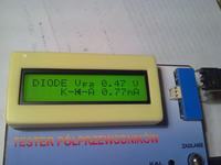

Link to original thread - Tester elementów półprzewodnikowych