Continue to Site

Welcome to EDAboard.com

Welcome to our site! EDAboard.com is an international Electronics Discussion Forum focused on EDA software, circuits, schematics, books, theory, papers, asic, pld, 8051, DSP, Network, RF, Analog Design, PCB, Service Manuals... and a whole lot more! To participate you need to register. Registration is free. Click here to register now.

Self cascoded differential pair transistors

Status
Not open for further replies.

Junus2012

Advanced Member level 5
Joined
Jan 9, 2012
Messages
1,552
Helped
47
Reputation
98
Reaction score
53
Trophy points
1,328
Location
Italy
Visit site
Activity points
15,235
Hello

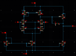
I see in some of design works some people are cascoding the input transistors of the differential pair transistors as shown in the attached image, they are arguing of giving better CMRR, which I don't understand why ?

secondly if this scheme is good as they say, why still not as a standared as simple differential pair, so what is the drawbacks behind this connection ?

Thank you in advance

casocdedif.PNG
 

I don't know why they call it a self cascoded transistor. This is simply a long composite transistor. It doesn't have the properties of a casoded transistor since the bottom transistor is in triode. If anything, it would be better called a degenerated transistor. It simply provides higher output resistance as any degenerated device will do.
 
I don't know why they call it a self cascoded transistor. This is simply a long composite transistor. It doesn't have the properties of a casoded transistor since the bottom transistor is in triode. If anything, it would be better called a degenerated transistor. It simply provides higher output resistance as any degenerated device will do.

Dear Suta,

Thank you for your reply,

regardless of the benefits, and as you said it is nothing but long composite transistor, for example, if I have one transistor with (W/L)= 10 µm/1 µm then I can build it with two transistors in series and (W/L) for each is 20 µm/1 µm, so as an equivalent ratio they are the same, then how their characteristics is different ??? like you also said the second one has degenerated
 

For one thing, the composite transistor gets a pole in the middle node. You can easily simulate one composite and one regular transistor side by side and compare the characterisitcs you are interested in.
 
For one thing, the composite transistor gets a pole in the middle node. You can easily simulate one composite and one regular transistor side by side and compare the characterisitcs you are interested in.

Dear Suta,

Thank you for your reply,

I have tried to simulate simple current mirror using composite transistors and non composed transistors, as shown below,
for the non composite mirror I chose W/L = 10 µm/1 µm and for the composite mirror I chose W/L = 20 µm/1µ for each transistor to give the same equivalent

circuit.PNG

As you said the bottom transistor for the NMOS will be in the triode region which provided me higher output resistance and hence more stable current as you see from the results below that show the output current of both mirror when I vary the output voltage

results.PNG

I have also tried to make composite differential pair of the two stage amplifier, that improved the gain a little, the circuit is shown below

opamp.PNG

for me the best result I am optaining when both composite transistors are with the same size, some people are suggesting to make the composite transistor at the drain terminal m times bigger than other transistor, what is the advantagues ? and I have tried it

but I didnt see an advantagues

Thank you once again
 

I always make them the same size. The only thing I can think of if you make the top transistor bigger in size (bigger W) compared to the bottom one is that now the Vgs for the top transistor is smaller for the same current. This means that the Vds of the bottom transistor is bigger and although it is probably still in triode, it will be getting closer to saturation, which means more degeneration for the top one. Or if it gets really at the edge of saturation then you have something that's similar to a cascode situation.
 
I always make them the same size. The only thing I can think of if you make the top transistor bigger in size (bigger W) compared to the bottom one is that now the Vgs for the top transistor is smaller for the same current. This means that the Vds of the bottom transistor is bigger and although it is probably still in triode, it will be getting closer to saturation, which means more degeneration for the top one. Or if it gets really at the edge of saturation then you have something that's similar to a cascode situation.

Dear Suta,

Thank you for your reply, indeed what you think is completely right and I found some designers and papers making the top transistor (for the NMOS composite) much more bigger than the down one in the attempt to make them both working in the saturation, I have tried it but either the top one leave the saturation and enter the subthreshold condition, or if it is succeed then the results I am getting by making them equal is still better, so why I should pay more area if the change is even worse,

Therefore, if I am going to cascode I will cascode with equal size as you do as well.

While this technique is giving observable advantages in current mirror, I have by simulation noticed that advantagues is not that much to do cascoding for the differential pair transistor, I have simulated it with the two stage op-amp, it only increases the gain with 1 dB, but the offset voltage was reduced

You have mentioned that when the down transistor is in the saturation then the transistor is more degenerated, why ?

Also could you please explain me how the down transistor is becoming in triode while the upper one in saturation ? asume NMOS composit with equal size transistors

Thank you once again
 

First question: imagine you have a source follower with the transistor connected to the source of the main MOS working as current source. Now, this configuration repeats the input signal at the source, but if you decide to connect some load at the drain and get a signal out of the drain like in a common-source, you will get nothing because you have huge degeneration at the source,caused by the current source there. Basically, to get a signal at the drain you need ac drain current going into the load but you can't have an ac current because the current source prevents any current fluctuations. Similar in the case of self-cascoded transistor if the bottom one is in saturation - it provides bigger degeneration.

Second question: the drain voltage of the bottom device is Vgs below input. And the input is somewhat bigger than Vgs needed for the current that the composite transistor works with. So the Vds of the bottom device is not that big and when it is below Vov, then the transistor is in triode, which is usually the case.
 
I don't know why they call it a self cascoded transistor.

Maybe it's a (somewhat obscure) abbreviation for self-biasing cascoded transistor. The upper transistor(s) need their own p-in-nwell substrates, which they bias themselves.
 
Maybe it's a (somewhat obscure) abbreviation for self-biasing cascoded transistor. The upper transistor(s) need their own p-in-nwell substrates, which they bias themselves.

Thank you Erikl,

As from my discussion with Suta, this configuration work fine if the both NOS have equal size and by doubling W for each we recover the original single transistor ratio with better performance, and although I downloaded a lot of papers of people making the drain transistor much bigger than the source transistor, but in my test was not showing the improvement, even with equal size is better,

Building the mirror with this scheme is improving the current source resistance and for differential pair it is improving the offset or the matching
 

Thanks a lot, Junus, for your summary. But you can be sure that I always read the whole thread before I answer. :smile:

Re. self cascoding I've seen similar results like you reported, then decided to never use it for differential amplifiers, because the small gain winnings aren't worth its effort (area costs), IMHO, particularly if the MOS are operated in weak inversion mode.

Re. less offset I'm not so sure if this is reproducible in layout. Other (geometrical) effects might cover or even dominate the self cascoding influence (for this s. also the contributions to your output offset voltage thread).


Thank you Erikl for your nice explanation and for sharing me your experience in this regard

Sure you know Johan Huijsing, the author of the Operational Ampliifer Theory and Design book, he published a lot of papers in Instrumentation Amplifier, he extensively used the composite transistors for the differential pair arguing that it will improve the CMRR, However, he is using low threshold voltage transistor for the composite transistor while the other one is normal MOS

Do you have a comment on this status :)

Thank you once again
 

Sure you know Johan Huijsing, the author of the Operational Ampliifer Theory and Design book, he published a lot of papers in Instrumentation Amplifier, he extensively used the composite transistors for the differential pair arguing that it will improve the CMRR, However, he is using low threshold voltage transistor for the composite transistor while the other one is normal MOS

Do you have a comment on this status :)

Hi Junus,

yes, I know his book and several papers by Johan Huijsing, very instructive ones, and I remember I've successfully used his class-AB output stage with its complementary floating current sources (e.g. Fig. 5.6.1 in his book) a few times.

Back to the differential pair with composite transistors (yes, that's a better term than self cascoded transistors, I think).
I didn't check its CMRR influence ('cause this was good enough anyway).

Usage of low VT transistors (if available) is equivalent to using a greater W/L ratio for the upper transistors: needing lower VGS (for the same current) results in higher Vds for the bottom transistors, so there's a fair chance to get them from triode into saturation region operation.
 
Status
Not open for further replies.

Part and Inventory Search

Welcome to EDABoard.com

Sponsor

Back
Top