moro
Member level 3

Hello,
i am working on a 4 layer pcb design on a circuit to drive a 3 phase bldc motor.
After some previous noise problems on my 2 layer design, i cam to the point where i want to go for a 4 layer.
So i have started working on the new pcb layout..
The goal is to minimize as much as possible the noise/ripple from the mosfet power stage, so it wont affect the control circuits
I started to follow this routing pattern
- top layer will provide +V for the power stage
- layer1 - will hold everything which is ground ( ground plane)
- layer2 - will hold some light power lines ( 5V, 3.3V and +12V for the FET drivers)
- bottom layer will hold the ouputs of the power stage
Right now i am focused on the ground layer, since i dont have galvanic isolation, everything is shared on the same ground net
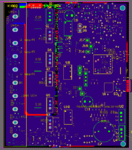
Bellow is a proposal i am thinking of, i wonder if there are any disadvantages between the bellow picture, and a fully filled layer


