Continue to Site

Welcome to EDAboard.com

Welcome to our site! EDAboard.com is an international Electronics Discussion Forum focused on EDA software, circuits, schematics, books, theory, papers, asic, pld, 8051, DSP, Network, RF, Analog Design, PCB, Service Manuals... and a whole lot more! To participate you need to register. Registration is free. Click here to register now.

Routing Eagle 7.6 TPA3122D2 Personal project

Status
Not open for further replies.

Zamfar021

Newbie level 4
Newbie level 4
Joined
May 30, 2016
Messages
7
Helped
0
Reputation
0
Reaction score
0
Trophy points
1
Activity points
45
Hello everyone,

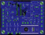
So this is my project :

View attachment 129437

I'm a new eagle user and am kinda stuck at the routing level.

I would like to use 1mm width. at 45°(wire bend style)
IC1 is 7812
IC2 is TPA3122D2.

Not sure how to use the auto-router option and honestly i prefer doing it manually.

Finally any advises or suggestions, on the placement of the components or any other mistake you might find? :thinker:

Feel free to ask any other info you might need.

Cheers,

5e73nt.jpg
new link.
 
Last edited by a moderator:

Hi,

It's difficult to review/improve placement without schematic.

Some recommendations:
* sooner or later you will use SMD. Why not now? Try a mixed design with some simple/easy_to_solder SMD devices to get familiar with SMD.
* do the placement with the schematic. Critical devices and paths first.
* Read the datasheet, especially device selection and layout considerations.
* bottom side = GNDplane
* use various trace width. 0.5 mm or smaller for signals, but thicker for high current paths.
* consider the paths for (pulsed) high currents..and back. They cause voltage drops =noise or distortion. Keep the length small, but use wide traces.

Klaus
 
And re-do your placement, highlight power and ground if possible and try different placements till you get the neatest looking RATs Nest of connections... PCB design is mostly placement so play about with it and look at the resultant pattern of connections and picture how they will route.
 
Hi again,

I have been trying hard.
the GND wire is hidden.

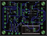
latest board i designed :

asdasd.JPG

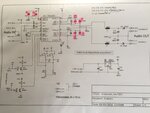
Schematic :

IMG_0089.JPG

Please Do tell what do i miss? :D
Thanks !
 

Hi,

There are some issues:
* IC2, pin1 is not connected to supply
* Q1 is mirrored
* place C14, C15, C16, C17, C18 close to their IC pins. Also the electrolytic capacitor placement could be improved.

Minor issues:
* You interchanged the placement of the components of right and left channel. This makes layout more difficult.
* if you route signals of IC2, pin 3 and pin6 on the left side, you have room to route the missing supply connections.
* try to make the traces for power supply and output signals more wide. They carry a lot of (pulsed) current. (This is more easy with corrected R and L placement)

Klaus
 
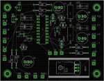
So far i keep failing, the last pic i shared didn't work out so well so i started all over again.
had difficulties to get the GND all over the board, too much cross routes....

the placement of components indeed.
asdasdasdasd.JPG
Can any1 help me with this? getting tired :bang:
 

Hi,

I think it was not too bad.

There are some issues:
* IC2, pin1 is not connected to supply
* Q1 is mirrored
* place C14, C15, C16, C17, C18 close to their IC pins. Also the electrolytic capacitor placement could be improved.
You did no improvement on these points.

If you don't correct the first two points your circuit won't work.

KLAUS
 

Hello again.

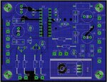
asdasdasdasdasd.JPG

this is my progress so far,

Can i share my project file here? should I?

Thanks in advance

- - - Updated - - -

Finaly ! :O Any observations?
asdhfghygjgtyjghymjknnnnnnnnnnnnnnnnnnnn.JPG
 

Hi,

It really isn't that hard.

First: complete the schematic. Now for the third time:
There are some issues:
* IC2, pin1 is not connected to supply...
--> instead of connecting pin1 ...now it seems you disconnected pin10.

Do you want your circuit to work? Then connect them.

********
Constraint:
Till now I thought you want a two layer design....now it seems you want a single layer design.
--> I strongly recommend to use two layers. One side GND (mostely), the other side signal routing.

*****
Placement. Critical signals / parts first.Try to remove signal crossings.

...
Then routing. Critical signals first.
Different trace widths.

******
You may add your project as an zipped attachment.

****after your update****
Now pin1 is connected, but not pin10.
Why the diversions? Keep the signals short.


Klaus
 

Updating :
 

Attachments

  • 06_14_2016.rar
    11.4 KB · Views: 119

Status
Not open for further replies.

Part and Inventory Search

Welcome to EDABoard.com

Sponsor

Back
Top