Continue to Site

Welcome to EDAboard.com

Welcome to our site! EDAboard.com is an international Electronics Discussion Forum focused on EDA software, circuits, schematics, books, theory, papers, asic, pld, 8051, DSP, Network, RF, Analog Design, PCB, Service Manuals... and a whole lot more! To participate you need to register. Registration is free. Click here to register now.

Routing a 20 pin BGA in Altium

Status
Not open for further replies.

Shannon_H

Newbie level 3
Newbie level 3
Joined
Mar 17, 2015
Messages
4
Helped
0
Reputation
0
Reaction score
0
Trophy points
1
Location
Moorhead, MN
Activity points
32
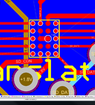
So I've used Altium for a little while for smaller projects (mostly through-hole components) and now I'm delving into surface mount components. When I try to route a 20-Pin Ball Grid Array I can't route the inner 4 pins. The only way I've been able to is by making my traces extremely thin. Is this the only way to get past the outer "wall" of pins or is there something special I should be using?
 

Attachments

  • bga question.png
    bga question.png
    77.5 KB · Views: 126

Last edited:

I started to do that after posting and I've found the fanout method is used a lot just like you said, yet my component has a very small pitch (0.4mm). I can make thin traces to go between the outer layer. What should I look out for if I have traces smaller than 0.1mm?
 

0.5 mm and 0.4 mm grid BGAs need typically technologies like microvias in BGA pad.

Fan-out with 50 - 70 µ traces is a theoretical option for BGAs with few pins like the present one. Main problen is risk of solder shorts. I presume this are soldermask defined pads, so there's very little overlap of traces and soldermask, a small mismatch would expose the traces.
 
You must be aware that the most critical requirements will limit the range of PCB manufacturers with which you can work.
 

If it is multiple layer PCB then you need to try via and pad. Which is like placing a via on pad itself and route from another layer. But you need to consider so many rules while doing this and also it will also increase your PCB fabrication cost.
 

Still undetermined. Currently I'm only working with top and bottom but I can add extra layers if need be.
 

If there are no other BGA devices on the board than the one presented in the previous image, a 2 layer PCB is quite enought for route it.
 

Then continue with 2 layers of PCB it will be more than enough for your circuit I guess.
 

I believe the discussion about number of layers is missing the point. The primary problem is which PCB technologies allow to route a 0.4 mm or 0.5 mm BGA at all. If you go for microvias, restrictions of via length apply, it may be unsuitable to use through-vias for fanout.
 

I would recommend searching a more convenient package for this part (such as TSSOP or QFN) if it's the only fine BGA in your design, otherwise manufacturing costs will be exuberantly high due to the small clearance and width constraints of this single part.
 
I have had boards done with very small PTH holes that have been filled and levelled and form the BGA pad for simple boards with these devices on.
What is the land size of the device.
 

This is actually the route we decided to take. Ended up finding a QFN which is MUCH nicer to route. Just had to do a bit more digging.
 

Status
Not open for further replies.

Part and Inventory Search

Welcome to EDABoard.com

Sponsor

Back
Top