Continue to Site

Welcome to EDAboard.com

Welcome to our site! EDAboard.com is an international Electronics Discussion Forum focused on EDA software, circuits, schematics, books, theory, papers, asic, pld, 8051, DSP, Network, RF, Analog Design, PCB, Service Manuals... and a whole lot more! To participate you need to register. Registration is free. Click here to register now.

ROM memory data reading

Status
Not open for further replies.

antlhem

Member level 1
Member level 1
Joined
Dec 8, 2016
Messages
41
Helped
0
Reputation
0
Reaction score
0
Trophy points
6
Activity points
364
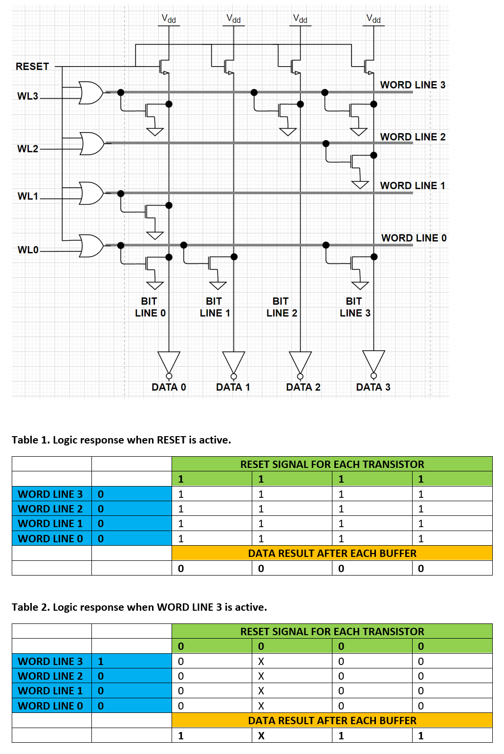
Hi. I am working out the reading data in a simple ROM, my question is, should I expect a don't care in "BIT LINE 1" when "WORD LINE 3" is active?
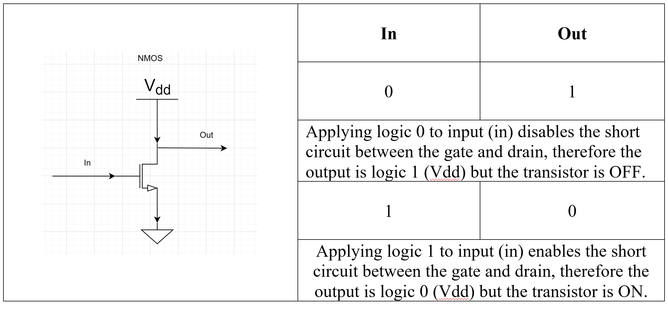
First, I show the basics about NMOS which are the transistors used in this diagram.
1604602076766.png

Then the small ROM diagram and tables that show the results when WORD LINE 3 is active.
1604602254515.png
 

Are these images from a textbook? The diagram shows 4 of everything. It's hard to be certain if all wiring is correct. Maybe someone other than the author drew the diagram and laid out the tables? And the artist made a mistake?

We'd have an easier time grasping what's going on if it were only 2 rows and 2 columns. Present the basic concept in the most basic manner.
Then extend to 3x3 array. Then 4x4.

Considering the article makes an immediate jump to 4x4, it would help if it printed the entire truth tables for all possibilities.
However the article only prints one sample truth table.

Did you try a simulation of this method?
 

Are these images from a textbook?
Hi, no is not from a text book. I did it my self and I following the principle of every time a word line is selected the Vdd will discharge through the transistor present in the word line, otherwise the Vdd will continue until the end, where the inverter will turn it into a logic zero. You can see this in the diagram below.
1604936570018.png

I am implementing this in Cadence, but the output remains zero all the time, even if I select a word line. Any suggestions on why this is happening?
 

Hi, I am making some tests with a simple ROM memory built with CMOS transistors. But each the output remains all the time the same. The selection of a word line should activate the available transistors in this line and discharge Vdd through them. Any suggestions on how to make this happen in this circuit?
The following diagram shows what should happen.
1604937105407.png


The following images are from Cadence software. This is the ROM and the results.
1604937236977.png
1604937284290.png
 

The schematic makes no sense. If the bit lines are tied permanently to Vdd, how could a transistor pull them down? You would either use a dynamic pull-up as in post #1 or a weak pull-up.
 

How is the reset in post #1 supposed to work? When reset = '1' you activate the pull-up for all data lines but also all the word lines.
It seems that you shouldn't activate both the pull-ups and all word lines at the same time.
 

    antlhem

    Points: 2
    Helpful Answer Positive Rating
I think I get the principle... Each transistor is a 'one'. In order for it to pull a bit wire low, there ought to be resistors at the top of bit wires just below each Vdd.
 

    antlhem

    Points: 2
    Helpful Answer Positive Rating
How is the reset in post #1 supposed to work? When reset = '1' you activate the pull-up for all data lines but also all the word lines.
It seems that you shouldn't activate both the pull-ups and all word lines at the same time.
Thank you, indeed I need resistors. One more question, please suggest me code in cadence to build bigger ROMs instead of doing it by hand. I would like to build 1 GB ROM or bigger.
--- Updated ---

I think I get the principle... Each transistor is a 'one'. In order for it to pull a bit wire low, there ought to be resistors at the top of bit wires just below each Vdd.
Yes I added the resistors, is working now. Thanks. Could you please suggest me code in cadence to build bigger ROMs instead of doing it by hand. I would like to build 1 GB ROM or bigger.
 
Last edited:

At each intersection where you have a transistor, you can substitute a diode (or led or zener diode). By turning on a word wire, a diode conducts to its respective bit wire.

Anyway it's easier than drawing transistors.

Schematic found at:

arith-matic.com/notebook/rom-ram-computer-memory

diodes on grid makes 4-bit ROM.png
 

At each intersection where you have a transistor, you can substitute a diode (or led or zener diode). By turning on a word wire, a diode

Could you suggest me a code to do this in Cadence-Virtuoso-Schematic? Instead of connecting one-by-one for bigger memories such as 1GB.
 

Does the software give you the option to write a script?... Consisting of FOR-NEXT loops which can put diodes at selected intersections? That's a labor-saving measure which makes it easier to fill a large array of memory.

Also be aware that the more components your schematic has, the greater the task for the simulator, reading a large file, running a simulation, making changes, etc.

And your task is made cumbersome working on a schematic that doesn't fit on one screen but requires scrolling up and down and across multiple screens.
 

Status
Not open for further replies.

Similar threads

Part and Inventory Search

Welcome to EDABoard.com

Sponsor

Back
Top