sameeksh shetty
Newbie

Hi ,
I am using zynq 7020 SOC for my fpga development.
In here there is a ADC device (ADC3660IRSBT) that is connected to fpga.
Few things on ADC configuration:-
1. The sampling rate is 10Mhz
2. Bandwidth we are targeting is 16 bit per channel.
3. We are using ADC in dual channel mode.
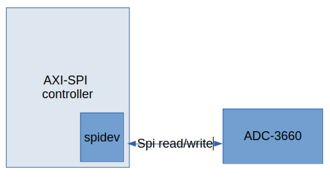
Now on FPGA side, we have created a IP for SPI controller. This IP communicated with ADC using spidev to configure,read and write into the spi device.

This has been achieved. We are able to configure the ADC and using the Integrated logic-analyzer we are able to see the data and clock pulse.
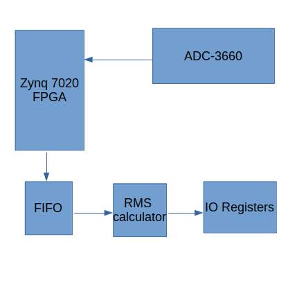
Now the next stage is data acquisition and calculation of RMS value. Here we though of storing the data that is coming in to be stored in FIFO block and then the RMS is calculated for the values stored in FIFO. This RMS value is then routed to IO registers.

I was not able to achieve this. I am unsure about this design idea.
So can you please any other way that has already been tried and tested .
Regards,
Sameeksh Shetty
I am using zynq 7020 SOC for my fpga development.
In here there is a ADC device (ADC3660IRSBT) that is connected to fpga.
Few things on ADC configuration:-
1. The sampling rate is 10Mhz
2. Bandwidth we are targeting is 16 bit per channel.
3. We are using ADC in dual channel mode.
Now on FPGA side, we have created a IP for SPI controller. This IP communicated with ADC using spidev to configure,read and write into the spi device.
This has been achieved. We are able to configure the ADC and using the Integrated logic-analyzer we are able to see the data and clock pulse.
Now the next stage is data acquisition and calculation of RMS value. Here we though of storing the data that is coming in to be stored in FIFO block and then the RMS is calculated for the values stored in FIFO. This RMS value is then routed to IO registers.
I was not able to achieve this. I am unsure about this design idea.
So can you please any other way that has already been tried and tested .
Regards,
Sameeksh Shetty
