Continue to Site

Welcome to EDAboard.com

Welcome to our site! EDAboard.com is an international Electronics Discussion Forum focused on EDA software, circuits, schematics, books, theory, papers, asic, pld, 8051, DSP, Network, RF, Analog Design, PCB, Service Manuals... and a whole lot more! To participate you need to register. Registration is free. Click here to register now.

Rigid flex Cross section OrCAD PCB Designer

Status
Not open for further replies.

jimmykk

Full Member level 3
Full Member level 3
Joined
Oct 2, 2014
Messages
158
Helped
0
Reputation
0
Reaction score
1
Trophy points
1,298
Activity points
2,865
Hi

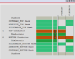
I am looking into designing a 2 layer rigid and 1 layer flex PCB on PCB designer 17.2. The rigid area is decided but the flex area is not completely decided yet. Here is the cross section:
crosssectin.PNG
crosssection1.PNG
As you can see, FLEXMAIN has a polyimide dielectric. So is it required to have polyimide dielectric in the rigid(PRIMARY) area as well? or is it ok this way?
If i go for Semi-flex(flex to install) PCBs and drop this FLEXMAIN(Flex) option, what layers have to be assigned to that? Would it only be copper(conductor) layer and soldermask flexible then?
 

I have designed several combined flex/rigid PCB, but your stack up drawing doesn't yet make sense to me. Usually the layers of the flex part (polyimide substrate, copper, coverlay in case of single layer flex) are continued into the rigid part.
 

I have to agree with FvM. It does not make sense.

Also, it is better to change the stackup to three copper layers, with the flex layer in the middle. This will make production much easier.
 

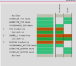
OK .....I edited the layers and now they look like like this:
cd.PNG
cd1.PNG
I made it with help of orcad rigid flex design practices: https://resources.orcad.com/3d-design-ecad-mcad-collaboration/rigid-flex-design-best-practices
I could not find any suitable reason that coverlay and adhesives should continue in rigid area. Maybe it has to do something with that my flex is single layer and in the mentioned paper it is double layered?
One question more is what gerber files need to be sent to manufacturer for rigid flex designs apart from : Solder Mask(top+ bottom), Assembly(T+B), Paste(t+b), top, bottom and internal layers. i.e.
are there any others than the usual ones
 

O.K., the coverlay and adhesive don't continue in the rigid part, but the flex substrate does. In so far your stack up looks better now. The stack up still doesn't look feasible at all. You have a polyimide soldermask defined for the rigid part which makes no sense. You should also consider that a copper layer below the polyimide substrate means to have a double side plated flex part, the bottom copper can be of course removed.

I understand now the notation of the PCB designer stackup.

Required gerber files are artwork respectively contours for all layers in the stack up. You can prepare an example set and send it to the PCB manufacturer to check if they understand it and are able to make it this way.

Some PC tools have difficulties to generate partial mask files (solder mask contains only the rigid part, coverlay the flex part), otherwise the PCB manufacturer need to separate the data.
 

Solder paste stencil for internal layers

Hi

I have a 4 layer (Top, Layer1, Layer2, Bottom) rigid board and the internal 2 layers(Layer1, Layer2) from this rigid pcb continue as flex PCB. I have to order a stencil for this board.

I can generate gerber files for solder paste top and bottom but i cannot find any pastemask_layer1 and pastemask_layer2 as there are some pads i need to apply solder paste on. So i was wondering which options i have to check here for generating the solder paste files for these layers.

c.PNG
 
Last edited by a moderator:

Thanks for reply....i made some changes and now i have 4 layers on rigid side and 2 layers on flex side.

The next problem is that i am able to get solderpaste_top and solderpaster_bottom gerber files for this stackup. But i also want solderpaste_layer(flex) and solderpaste_layer2(flex) as there are some pads on my flex design for which i want to order a stencil.
 

I would expect common stencils for rigid and flex part. A support may be required for the flex part.

Special problem is second printing pass. It may be difficult up to impossible, depending on the board geometry, component locations and component height of the first assembly pass.
 

Re: Solder paste stencil for internal layers

Maybe, just maybe, you should tell us what software you are using. Showing a picture of the dialog for selecting layer colors is useless. Maybe you need to check "pastemask_top" and "pastemask_bottom".
 

Solder mask and -paste are linked to top and bottom copper layer. You can't place component pads at internal layers and get no auto generated solder mask and solder paste for this layers, unless the PCB tool has an embedded components option.

It's however possible to draw all required structures manually and it's possible to get the intended Gerber files by manipulating the postprocess output in a Gerber tool or even in a text editor.
 

I am using OrCAD PCB Designer.....I have generated the usual rigid PCB Gerber files for all the layers.
But i have a question regarding: what else i need to deliver to the manufacturer. I see there is a rigid flex option in colors dialog, but i need some guidance regarding which other ART files need to be generated. I mean all the info regarding flex area, coverlay, adhesive needs to be in own ART files?
 

Your question has been answered generally before. Apparently you are planning some unusual features like SMD components on the flex part.

Beyond implementation in Orcad, you should have a stack-up sketch that shows how the finished board should look like. You should consider how the double sided SMD assembly can proceed, if you need a support or framing panel for pick-and-place.

It's not unusual to send preliminary data to the PCB house for clarification of non-standard stack-ups.
 

Status
Not open for further replies.

Part and Inventory Search

Welcome to EDABoard.com

Sponsor

Back
Top