Continue to Site

Welcome to EDAboard.com

Welcome to our site! EDAboard.com is an international Electronics Discussion Forum focused on EDA software, circuits, schematics, books, theory, papers, asic, pld, 8051, DSP, Network, RF, Analog Design, PCB, Service Manuals... and a whole lot more! To participate you need to register. Registration is free. Click here to register now.

RFID tag simulation at CST

yasemin_

Newbie level 5
Newbie level 5
Joined
Jan 29, 2025
Messages
8
Helped
0
Reputation
0
Reaction score
0
Trophy points
1
Activity points
85
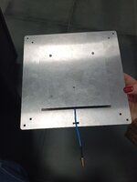
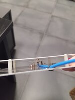
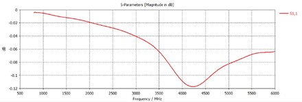
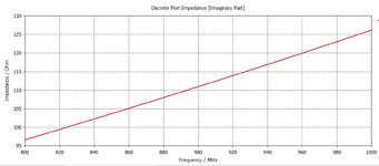
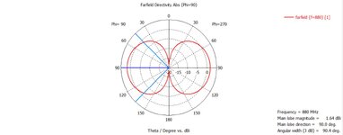
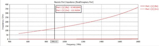
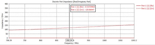
Hello, I am trying to simulate an RFID tag in CST. The structure in the image I attached is to match the impedance of the chip. I am trying to find the input impedance of this with simulation. I simulated it using discreate port but the impedance value I got is incorrect. Am I using the port wrong? The real component of the impedance I need to get for around 890 MHz is 0.22 ohms, the imaginary component is 120 ohms. But what I get is different. In addition to that I should get an omnidirectional radiation pattern, but this is also different. I can't find where I made a mistake.

WhatsApp Image 2025-01-29 at 08.30.31.jpeg
 
Which values do you get?

It looks like the lumped port is intersecting with the conductor crossover. You can build a small "metal bridge" to avoid that.
 
Which values do you get?

It looks like the lumped port is intersecting with the conductor crossover. You can build a small "metal bridge" to avoid that.
Thank you for your suggestion. I have attached the values I got and the radiation pattern. I don't know what kind of metal bridge I need and how I can do it. Is there a source about this?
 

Attachments

  • real.JPG
    real.JPG
    85.2 KB · Views: 32
  • imaginer.JPG
    imaginer.JPG
    89.9 KB · Views: 35
  • farfield.JPG
    farfield.JPG
    70.8 KB · Views: 30
That looks close, not bad. The pattern looks correct, these loops are not omnidirectional. The real part depends on conductor loss, so check your metal model. To tweak imaginary part (inductance) just tweak the size of the loop.

With bridge, I meant a bridge, but it seems that your model works ok as is.
This loop design belongs to my professor. He has already simulated it in CST and obtained the real and imaginary components of the impedance. The impedance value in the professor's simulation is consistent with our theoretical calculations. I expected to find the same impedance by taking the same loop design and simulating it, but mine is different. If I understand you correctly, it is not necessary to put a bridge, so what else could be the reason why I did not find the same impedance?
 
so what else could be the reason why I did not find the same impedance?
As FvM already mentioned, the difference might be in meshing.

Inductance is close, but you have more conductor loss, and both values are affected by skin effect, which must be modelled accurately.
Firstly, you need fine enough mesh density, have you checked result convergence with different mesh density?
Secondly, there are two methods for modelling such metal traces, either by equivalent surface impedance (no mesh inside metals) or by meshing into skin effect (mesh in conductors also). From my experience with other EM tools, for such cross sections it is more accurate to mesh inside the conductors as well, "solve inside" is the wording using in some other EM tools. Not sure what names CST use for this, but I hope you understand what I am talking about.
Thank you for your suggestion. I understand what you mean. The size of the loop is around 5 mm, which means a simulation time of 3 to 4 hours with the computer I use. Therefore, it is difficult for me to reach the result by playing with the parameters. I will repeat the simulation by reducing the mesh density and I will definitely share the result.
In addition to these, I would like to ask three more things as I don't know if they are effective or not.
1. I import this simulated loop as a DXF file. Then I enter the required thicknesses using the shape tools> Shell solid or thicken sheet tool. Then I make material definitions. Is there a problem with importing and simulating the loop with this method?
2. I am using time domain solver, should I use different solvers?
3. When defining the S-parameter discreate port, I use the impedance at the default value of 50 ohms. Am I doing it right? Or is there another value that the impedance should take?
 
Using the 50 Ohm default port impedance is fine.

Time domain solver is ok, but you can try the CST FEM solver to mesh into skin effect with adaptive mesh refinement. Personally, I would use EM simulation in ADS Momentum for this, which is optimized for such planar simulation tasks. This will give very accurate results in less than a minute.

If you upload the DXF file and provide the thickness and materials for conductor and substrate, I can run the model in my simulator to verify the results.
First of all, thank you for your support. I still haven't achieved the desired result, so I would love to get your help with the simulation. However, this design belongs to my professor; unfortunately, he did not allow me to share it.
I want to update you on the progress. As you suggested, I increased the mesh density. The imaginary component of the impedance reached the desired value of 120 ohms. However, the real component did not turn out as expected. Compared to the initial simulation results I shared, the real component has increased. Could this still be related to the mesh structure?

Additionally, there is something I don't understand. This loop is designed to match the impedance of the chip. The chip impedance is a complex number. I don’t understand why we choose 50 ohms when using a discrete port. After all, the system I am simulating does not operate at 50 ohms. Why do we use 50 ohms?
 
Could this still be related to the mesh structure?
When increasing mesh density, results should converge towards the "correct" results. If you have much higher series resistance, double check your material properties.

In my first answer, I had doubts if the lumped port is valid when it passes through the crossover metal. You could create a little bridge that goes up into air at the intersection, height above the trace crossover maybe 5 * metal thickness. I hope you understand this "brigde" task - just draw at little via at the ends of the trace that goes up into air, and connect the lumped port there.

Of course, your professor's result could also be wrong.

Additionally, there is something I don't understand. This loop is designed to match the impedance of the chip. The chip impedance is a complex number. I don’t understand why we choose 50 ohms when using a discrete port. After all, the system I am simulating does not operate at 50 ohms. Why do we use 50 ohms?

The port impedance matters when you look directly at the parameters.

When you insert the S-parameter data into circuit simulation, the simulation will "see" the correct impedance of the data block, no matter what reference impedance you had used for simulation. The simulator knows the impedance from the header of the S-parameter file, and uses that to calculate data.

If you want to do an experiment, you can take data simulated with different port impedances and convert them to [Z] or [Y] parameters - you always get the same result. The port impedance cancels out when you do that math, and doesn't have an effect.
 
When increasing mesh density, results should converge towards the "correct" results. If you have much higher series resistance, double check your material properties.

In my first answer, I had doubts if the lumped port is valid when it passes through the crossover metal. You could create a little bridge that goes up into air at the intersection, height above the trace crossover maybe 5 * metal thickness. I hope you understand this "brigde" task - just draw at little via at the ends of the trace that goes up into air, and connect the lumped port there.

Of course, your professor's result could also be wrong.


The port impedance matters when you look directly at the parameters.

When you insert the S-parameter data into circuit simulation, the simulation will "see" the correct impedance of the data block, no matter what reference impedance you had used for simulation. The simulator knows the impedance from the header of the S-parameter file, and uses that to calculate data.

If you want to do an experiment, you can take data simulated with different port impedances and convert them to [Z] or [Y] parameters - you always get the same result. The port impedance cancels out when you do that math, and doesn't have an effect.
Hello,
I have checked the material properties, and they are the same as the ones used by my professor. The theoretically calculated impedance of this loop is also very similar to the impedance my professor found. Therefore, we believe that my professor’s results are correct.
As you suggested, I added a bridge to the trace ends. When you mentioned a “bridge,” two different designs came to my mind, so I tried both. Maybe both are wrong☹
For the first bridge, I considered it as a conductive wire. I have attached an image of this design. The impedance of this bridge was 0.54 (real) and 122.91 (imaginary). For the second bridge, I considered it as a copper structure rising from the loop. I have also attached an image of this design. The impedance for this bridge was 0.53 (real) and 120.069 (imaginary). Are these bridges incorrect?
 

Attachments

  • bridge1.jpeg
    bridge1.jpeg
    52.8 KB · Views: 20
  • bridge1_imp.jpeg
    bridge1_imp.jpeg
    91.9 KB · Views: 19
  • bridge2.jpeg
    bridge2.jpeg
    51.8 KB · Views: 28
  • bridge2_imp.jpeg
    bridge2_imp.jpeg
    91.3 KB · Views: 27
For the second bridge, I considered it as a copper structure rising from the loop
This is what I meant, looks good to me!

You now get the exact imaginary part that you wanted to have, 120 Ohm which equals 21.5nH. That is an excellent agreement.

Only the losses are higher than your professor simulated, but both values look reasonable. If your metal definition agrees, and your mesh is fine enough, my only idea is that your simulation boundaries are too close and cause eddy currents in the boundary condition. But this should also be visible in imaginary part, so I think this is not your issue. I would place the simulation boundaries at least 1 inductor diameter away, then it has very little effect.

From my viewpoint as an RF simulation expert, your results look reasonable and your professor should tell you what he might have done differently to calculate series resistance. I have see more than one professor creating terribly wrong simulation models ...
I was worried that it might be incorrect, so I’m glad to hear that it’s right! I put a lot of effort into this simulation, and thanks to your guidance, I was able to reach a solution. Thank you very much!
These simulations are part of a project led by my professor. I want to work with him on this project, and he told me that if I manage to complete a few simulations, he would let me join. However, I’m a beginner when it comes to simulations, so I’m struggling. Additionally, finding resources on RFID system simulations is quite difficult.
Maybe I should have started a separate thread for this, but since I’ve come across an expert like you, I didn’t want to miss this opportunity. I have another simulation problem ☹

The second thing I need to simulate is the antenna I shared a photo of. The antenna feed is as follows: the inner conductor of the coaxial cable is soldered to the top plate, while the shield is connected to the bottom plate. I modeled the antenna in CST and also attached images of my model. I tried to make the model resemble the structure in the photo. I positioned the inner conductor so that it touches the top plate, while the shield does not touch the top plate but connects to the bottom plate. Finally, I created a waveguide port at the end of the coaxial cable. I hope I was able to explain what I did.

My professor said that this antenna should have a resonance frequency of 910 MHz. However, my simulation results are a disaster 😊 Where did I go wrong this time?
 

Attachments

  • AntennaPat1.jpeg
    AntennaPat1.jpeg
    630.9 KB · Views: 24
  • antennaPat2.jpeg
    antennaPat2.jpeg
    431.2 KB · Views: 26
  • antenna1.JPG
    antenna1.JPG
    20.8 KB · Views: 26
  • antenna2.JPG
    antenna2.JPG
    33.2 KB · Views: 27
  • antenna3.JPG
    antenna3.JPG
    37.6 KB · Views: 24
  • S11.JPG
    S11.JPG
    76.6 KB · Views: 26
The second thing I need to simulate is the antenna I shared a photo of.
I think you should open a spearate topic, so that others can jump in who have more CST-specific experience than me.

From what I can see, you have not modelled the real geometry at the coax feed, where the coaxial feed ends on that U-shape connected to the bottom. From there, you only have the center pin (without dielectric and shield) connecting to the top plate (radiator).

In "my" EM simulator (Empire XPU) the coax port can have a center pin that stands out from the end of the coax. Not sure if CST has that as well, otherwise just model a metal cylinder for that center conductor section between coax end and top plate.
Sure! Here's the translation:


I didn't realize that not modeling the U-shaped connection point could have such an impact. I will update the model accordingly. Thank you for your support!
 
I didn't realize that not modeling the U-shaped connection point could have such an impact.
I don't know if this is the only problem, but the length of the "only center pin" section between end of coax and the top plate is different with the U-shaped design.

Another difference in your model is the isolation post: in the hardware, they end at the top and bottom plate, and do not cut big holes through the metals.


Write your reply...

LaTeX Commands Quick-Menu:

Part and Inventory Search

Welcome to EDABoard.com

Sponsor

Back
Top