Continue to Site

Welcome to EDAboard.com

Welcome to our site! EDAboard.com is an international Electronics Discussion Forum focused on EDA software, circuits, schematics, books, theory, papers, asic, pld, 8051, DSP, Network, RF, Analog Design, PCB, Service Manuals... and a whole lot more! To participate you need to register. Registration is free. Click here to register now.

RF PCB design in altium

Status
Not open for further replies.

leaps

Member level 2
Member level 2
Joined
Jul 10, 2008
Messages
53
Helped
1
Reputation
2
Reaction score
0
Trophy points
1,286
Activity points
1,620
hello everyone I am a newbie PCB design using altium, I am designing PCB for amplifier circuit at 80MHz for the circuit I am using surface mount components. I need some feedback with the fallowing questions as I am new to this

1- How does one determine the optimum height of board material

2- I have substrate height on 20 mils, Er=3.55 for Zo=50 ohms I get width of 44.8 mil and I have been told line widths more than 20mils is not recommended so what should I do my surface mount components are 0603m/0805in/2520mm.

3- I am aware RF signal path line has to have a width for a 50ohms line but the lines connecting for DC bias components can have different width??

4- what is the recommended spacing between smd inductors connected in series?

5- how do i determine the optimum width of signal trace on the bottom layer
 

3- I am aware RF signal path line has to have a width for a 50ohms line

Line width matters if the lines have a relevant length compared to the wavelength. At 80MHz, where your routing length is most likely < 1/20 wavelength, there is no need for controlled line impedance.
That said, you should keep your interconnects between SMD components short, and to avoid parasitic series L and parasitic shunt C. Make it small, that's the rule.
 
  • Like
Reactions: leaps

    leaps

    Points: 2
    Helpful Answer Positive Rating
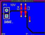
volker@muehlhaus thanks I am using bottom layer for dc supply distribution. the separation between Vdc is 20mil how do i determine its optimized any suggestions
a- bottomlayer.jpg

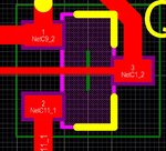
Also is it ok to route the RF signal under Q.
b-two.jpg
 

Slots in the ground will cause return current to flow a much longer path, that's bad. You can solve this by placing a suitable capacitor (1nF or so) across the slot, so that RF current can flow on the ground layer underneath the RF trace.
 

routing length is most likely < 1/20 wavelength, there is no need for controlled line impedance.
That is too big a constraint. Controlled line impedance starts at more than 1/4 wavelenght.. Why do you use that number ?
 
  • Like
Reactions: leaps

    leaps

    Points: 2
    Helpful Answer Positive Rating
That is too big a constraint.

I know ... used this number to indicate that it's really no issue here. The usual estimate for line effects (include or ignore) is lambda/10, calculated using the effective wavelength in that substrate.

Controlled line impedance starts at more than 1/4 wavelenght..

Wrong. At lambda/4 it doesn't start, at lambda/4 you are in massive trouble already because an open end converts into an RF short.
 
Hi I have a fallow up question I need to use conductor's as RFC's and how do i chose between shielded inductor vs unshielded one and layout considerations for both
 

Status
Not open for further replies.

Part and Inventory Search

Welcome to EDABoard.com

Sponsor

Back
Top