Continue to Site

Welcome to EDAboard.com

Welcome to our site! EDAboard.com is an international Electronics Discussion Forum focused on EDA software, circuits, schematics, books, theory, papers, asic, pld, 8051, DSP, Network, RF, Analog Design, PCB, Service Manuals... and a whole lot more! To participate you need to register. Registration is free. Click here to register now.

RF Board Design Guide

Status
Not open for further replies.

x4ce

Newbie
Newbie level 4
Joined
Dec 31, 2009
Messages
5
Helped
0
Reputation
0
Reaction score
0
Trophy points
1,281
Location
Pakistan
Activity points
1,329
Hi,

I am an amateur in the field of PCB design and my experience includes multiple PCBs design of basic digital electronics and STM microcontrollers etc. I have got them manufactured by JLCPCB and they worked, successfully. This is my first basic RF PCB designed in KiCad and requires some guidelines before I go for assembly etc.

The frequency signals range from 250 to 500MHz.

What I know and have done so far:

The lengths of traces carrying the high-frequency signals should be shorter than 1/10 of the wavelength of the highest frequency taking into account the propagation delay due to PCB.

The traces for high-frequency signals should possibly remain straight or should have a radius of curvature.

The width of high-frequency signals should be 3mm in order to match the impedance of 50ohm for PCB of 1.6mm thickness & FR 4.6.[/li][/list]


The guidelines required are:

1. Is the ground fill zone/ place fine on the top layer with RF signals?
2. If ground fill/ plane is not required on the top layer then I need to put via holes for ground pads. Any criteria for this? There should be at least 2 via holes? Distance between them etc.?
3. The pads etc. do no match the trace width (0.3mm), would they affect the impedance matching, and, if so, what is the solution?
4. Should I place a guard ring around the whole PCB or between the input and output antennas?[/li][/list]

I have attached the initial PCB design with component detail on the silk screen for ready reference.

I will be grateful if someone could guide me.

Regards
Shahid
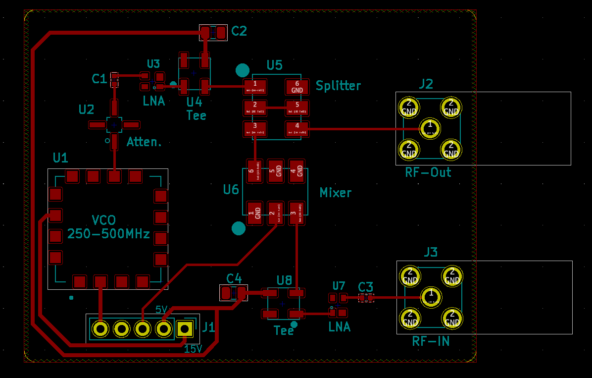
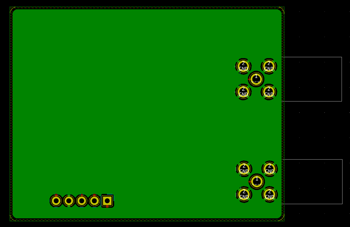
Screenshot_15.png
Screenshot_16.png
Screenshot_17.png
 

3 mm wide traces - where?

1/10 lambda rule doesn't apply to matched impedance traces.

Ground planes should be shorted by multiple vias, otherwise you have to expect resonances

Flooding the top side with copper changes transmission topology from microstrip to coplanar strip with ground, impedance calculation is different and depends also on copper pour clearance.
Coplanar is a possible way to achieve 50 ohms impedance on a thick two layer PCB, but not with the shown dimensions.
Thanks for replying.

Sorry, I meant 0.3mm trace width.
It is one of my concerns that should I have top ground fill plane or not. Yes, you are right it will make coplanar topology. So, you suggest, I should remove ground plane from top and use via holes on pads to connect them ground. Along with use evenly distributed via holes on top to ground to avoid resonance?


Thanks
 

Impedances according to Saturn PCB Toolkit

1665643646099.png
1665643699089.png

--- Updated ---

You need 1 - 1.2 mm trace width to achieve 50 ohm in coplanar waveguide topology. Get slightly different result with other tools, but Saturn Toolkit is basically reliable. It's free, do your own calculations.
 
Hi,

I just want to emphase: (for the OP but other members as well)
For both cases the GND plane really needs to be solid: No cut underneath your "signal trace", no other signals underneath your signal trace.

Solid as shown in your last picture of post#1.

Klaus
 
Impedances according to Saturn PCB Toolkit

View attachment 179074 View attachment 179075
--- Updated ---

You need 1 - 1.2 mm trace width to achieve 50 ohm in coplanar waveguide topology. Get slightly different result with other tools, but Saturn Toolkit is basically reliable. It's free, do your own calculations.


Hi,

In order to keep traces thinner and to avoid complexity, I have designed a 4-layer PCB with following stack-up:

1 - Signal
2- Ground
3 - 5V
4 - Signal

The height between first 2-layers i.e. RF components and ground is 0.2104mm which gives approximately 0.3mm trace width for 50ohm match. The VCO is 250-500MHz and I think it is not much high frequency and I've kept the RF signal trace lengths smaller.

Please have a look and suggest any improvement or issue you see. Moreover, should I place a guard ring around RF components?

Thanks
Shahid

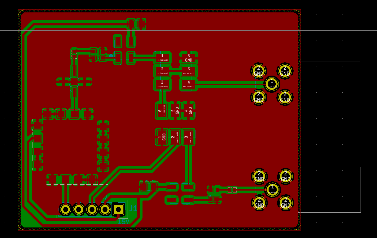
lay3_5v.PNG
lay2_ground.PNG
lay1_RF.PNG
 

Hi,

I am an amateur in the field of PCB design and my experience includes multiple PCBs design of basic digital electronics and STM microcontrollers etc. I have got them manufactured by JLCPCB and they worked, successfully. This is my first basic RF PCB designed in KiCad and requires some guidelines before I go for assembly etc.

The frequency signals range from 250 to 500MHz.

What I know and have done so far:

The lengths of traces carrying the high-frequency signals should be shorter than 1/10 of the wavelength of the highest frequency taking into account the propagation delay due to PCB.

The traces for high-frequency signals should possibly remain straight or should have a radius of curvature.

The width of high-frequency signals should be 3mm in order to match the impedance of 50ohm for PCB of 1.6mm thickness & FR 4.6.[/li][/list]


The guidelines required are:

1. Is the ground fill zone/ place fine on the top layer with RF signals?
2. If ground fill/ plane is not required on the top layer then I need to put via holes for ground pads. Any criteria for this? There should be at least 2 via holes? Distance between them etc.?
3. The pads etc. do no match the trace width (0.3mm), would they affect the impedance matching, and, if so, what is the solution?
4. Should I place a guard ring around the whole PCB or between the input and output antennas?[/li][/list]

I have attached the initial PCB design with component detail on the silk screen for ready reference.

I will be grateful if someone could guide me.

Regards
Shahid
I recommend Megtron6 PCB material for RF PCB design to safe you from signal distortion in the future
 

-There is no Top-to-GND via. Place stitching vias where possible.
-Use Microstrip/Co-Planar line rules for impedance matching.
-Don't use thermal relief for connectors' GND connections. Instead use direct connection.
-Don't place critical components at long distance, instead make them closer possible.

-There is no Top-to-GND via. Place stitching vias where possible.
As another member said above:

For both cases the GND plane really needs to be solid: No cut underneath your "signal trace", no other signals underneath your signal trace.

Solid as shown in your last picture of post#1.

Klaus

So placing stitching vias won't affect this as it will be on the sides of traces?

I will put the other suggestion before manufacturing....

Thanks
 

Hi,

I don´t see your concern.

Like FvM said, there are:
* Microstrip (GND plane, signal on different layer, no GND along the signal on the same layer)
* Coplanar waveguide (GND plane, signal on different layer, GND along the signal on same layer)

For coplanar waveguides you may use stiching vias.
But in both cases you need the very solid GND plane.

Klaus

Hi,

Thanks for the guidance and as I am using microstrip topology so there is no need of stitching vias.

Shahid
 

Status
Not open for further replies.

Part and Inventory Search

Welcome to EDABoard.com

Sponsor

Back
Top