Continue to Site

Welcome to EDAboard.com

Welcome to our site! EDAboard.com is an international Electronics Discussion Forum focused on EDA software, circuits, schematics, books, theory, papers, asic, pld, 8051, DSP, Network, RF, Analog Design, PCB, Service Manuals... and a whole lot more! To participate you need to register. Registration is free. Click here to register now.

Relating OP-amp block with equivalent transistor model

Status
Not open for further replies.

engrMunna

Advanced Member level 4
Full Member level 1
Joined
Oct 25, 2010
Messages
106
Helped
6
Reputation
12
Reaction score
5
Trophy points
1,298
Activity points
2,071
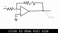
When analysing op-amps as a block diagram like in fig1 we say that because node B is at ground so node A will also be at ground
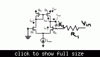
but when i look at the equivalent model of the op amp at transistor level in fig 2 I can't see how making Vin- ground will
make Vin+ at ground too??

And the second thing I dont get is that if in fig2 Q1 gate is grounded (small signal ground) wont this make Vgs (small signal) negative.
Thanks
 

Here is shown whole model of OpAmp circuit (Ic 741 )
see s. 25...35.


**broken link removed**

KAK
 

thanks for the reply, yes I saw the slides from pg 25 to 35 but my question is still un answered, how does the gate of one input transistor have the same potential as that of the gate of the other input transistor? i mean HOW?
 

When analysing op-amps as a block diagram like in fig1 we say that because node B is at ground so node A will also be at ground
but when i look at the equivalent model of the op amp at transistor level in fig 2 I can't see how making Vin- ground will
make Vin+ at ground too??

Both circuits are different and cannot be compared. The first one consists of a high gain amplifier with negative feedback and the second one is a simple differential amplifier without feedback.
Please note that the rough estimate VA=VB for the opamp inverter is only an assumption that results from the very large gain of the opamp unit (1E4---1E6). This assumption is helpful for calculation purposes only and may be used in case of negative feedback only.
 
You said the second figure doesnt have any feedback....but doesn't the resistor from output to the gate compose a feedback path?
I thought that for positive and negative both type of feedback we could consider the input terminals at the same potential....i didnt know that we do that only for negative feedback thanks
 

You are right, sorry. I have overlooked the resistor R2 that - indeed - establishes negative feedback (in a relatively uncommon configuration).
Nevertheless, for the opamp as well as for your cicuit the voltage difference between both inputs never disappears.
That means, the concept of "virtual ground" is only an approximation and a simplification for calculating purposes.
Due to the negative feedback (NOT for pos. feedback) the difference is determined by the open loop gain - resulting in some microvolts in case of opamps.
 
I forgot to mention that - in contrast to the opamp case - the feedback path R2-R1 will destroy the operating point because the collector dc voltage is not zero (other as the output voltage for opamps).
 

Status
Not open for further replies.

Similar threads

Part and Inventory Search

Welcome to EDABoard.com

Sponsor

Back
Top