Continue to Site

Welcome to EDAboard.com

Welcome to our site! EDAboard.com is an international Electronics Discussion Forum focused on EDA software, circuits, schematics, books, theory, papers, asic, pld, 8051, DSP, Network, RF, Analog Design, PCB, Service Manuals... and a whole lot more! To participate you need to register. Registration is free. Click here to register now.

Regulation Path for NCP1937 & NCP4355

Status
Not open for further replies.
Newbie level 3
Joined
Jun 20, 2023
Messages
4
Helped
0
Reputation
0
Reaction score
0
Trophy points
1
Activity points
38
Hi! I'm doing a SMPS of 120W using a reference design from onsemi NCP1937BADAPGEVB.

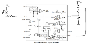
I did a lot of reverse engeneering in this design due to lack of information provided in the datasheet of NCP1937, although it has 40 pages. To achive regulation, NCP4355 (U4) is the solution provided by de reference design. In the regulation path, an optocoupler (U2) is connected to FBB pin in NCP4355, which drives a current that comes from an OTA. This OTA is controlled by a diferential voltage, which is a reference voltage and the output voltage scaled.

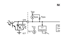
So if the voltage goes up, a current will start increasing at the diode of U2, and therefore the IC of phototransistor too. This current is very important because, sets the voltage at QFB pin in NCP1937 by R24, and with the internal components (IQFB, RQFB, VDD). The problem is that voltage at this pin could swing between 4.1V and 0.4V when is Vo at nominal load and Vo at minimum load, and that excursion is a delta current in the phototransistor in the order of micro amps. This means that current sinking from the OTA is in the order of micro amps too, giving a delta Vo in the order of micro volts. Datasheet of NCP4355 specifies that minimum current at OTA in regultion is at least 2mA. So how is this possible?

Thanks in advance.
 

Solution
Yes, the behaviour of NCP1937 is simulated with a machine state in LTSpice and the model of phototransistor is the one Im using.

My partner and I just figured out that the OTA controlling the feedback loop in NCP4355 has and active integrator with a feedback capacitor placed between VSENSE and IFBC Pin. This causes to reject the ripple from vout. So case solved.

Thanks again!
At NCP4355 datasheet. Table "Electrical Charecteristics" ->VOLTAGE CONTROL LOOP OTA -> Sink Current Capability.

I was able to simulate the feedback loop with the optocoupler, and Vout stays at 24V with very very low ripple, but this minimun ripple makes the voltage at ncp1937 VQFB to swing from 4,17V to 0.4V, and that makes no sense because this pin in regulation is intended to use it as feedback when you change load, and the valley at which primary controller swichs on is controlled by this pin. I attach some images for better understanding.

LTSpice Simulation.PNG


Swing VQFB.PNG


Ripple Vout.PNG
 

Attachments

  • Waveforms in NCP4355.png
    Waveforms in NCP4355.png
    40.6 KB · Views: 89
  • Internal Circuit of Regulation in NCP4355.png
    Internal Circuit of Regulation in NCP4355.png
    117.4 KB · Views: 107
  • Internal Circuit of QFB.png
    Internal Circuit of QFB.png
    25.4 KB · Views: 108
  • Regulation Path.png
    Regulation Path.png
    481.1 KB · Views: 120
Last edited:

At NCP4355 datasheet. Table "Electrical Charecteristics" ->VOLTAGE CONTROL LOOP OTA -> Sink Current Capability.
Right, I think by "capability" it means the maximum current it can sink, not the minimum for regulation. I don't see it clearly stated anywhere that there is a minimum FBC current.
 

Yes, that makes much more sense.

My question was more about the sensibility of the feedback loop controlled by NCP4355. I was able to simulate this as it Is showed un attached images, and very little ripple in Vout (due to Cout) Is capable of making voltage at VQFB in 1937 swing from 4v to 0.4v, meaning that the controlled is hopping valleys with the same load.

I understand that this pin is for detecting changes in load, but the analysis of the reference design i made, shows the behaviour described above. So i dont understand in the reference design, how Is possible that ripple in vout (maintaining the load) has negglible effect on VQFB pin at 1937.


Thanks in advance,
 

Yes, I was just correcting a minor misunderstanding. But I think I understand your overall doubts. I don't have much familiarity with these chips, or any spice models to try, but can do some rough math.

Seems like in your simulation the loop gain is too high. Are you sure your models for the NCP4355 and ncp1937 are accurate? Also did you check the gain of the phototransistors? I can't even tell what part numbers U2 and U3 are....
 

Yes, the behaviour of NCP1937 is simulated with a machine state in LTSpice and the model of phototransistor is the one Im using.

My partner and I just figured out that the OTA controlling the feedback loop in NCP4355 has and active integrator with a feedback capacitor placed between VSENSE and IFBC Pin. This causes to reject the ripple from vout. So case solved.

Thanks again!
 

Solution
Status
Not open for further replies.

Similar threads

Part and Inventory Search

Welcome to EDABoard.com

Sponsor

Back
Top