Vermes
Advanced Member level 4


The generator was originally made in the 80s-90s of last century. Its assumptions were the following:
- generation of waveforms shaped triangle, rectangle and sine
- output frequency from 0,1Hz to at least 1MHz
- the possibility of sweeping the internal and external signal
- implementation on widely available, popular discreet elements (transistors, integrated circuits) without using dedicated circuits type XR2206 or ICL8038
- attempt to use a commercially available integrated circuit line receiver TTL type UCY75107
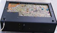
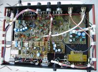
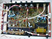
Schematic diagrams after modifications:
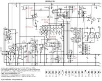
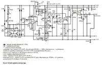
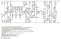
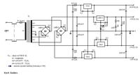
This generator operates on the classical principal of charging and discharging the capacitor with current of the stabilized value.
Adjust the frequency in each range is x11 and is implemented by changing Uwe range 0,182 to 2,00V, which translates into a charge current 2 to 22mA, and the discharge current 4 to 44mA.
Charging current flows into the capacitor all the time, while discharge current is switched by the comparator, when it detects a peak reaching +2,25V voltage and is switched off when the voltage reaches a lower peak of -2,25V.
A general description of the system:
IC1 and IC2a move Uwe to -5V level, the inverter on IC2b and T1 moves Uwe to +5V level with reversed phase. IC3b and T2 is the key L (loading). IC4 and T3 is the key R (discharge). IC5 – the comparator, T3-T4 is on/off the key R. IC6 is a buffer – amplifier for the triangle-sine converter.
Motherboard 2 sided (printing painted with spirit lacquer). There is the whole system with the exception of the control voltage in the form of separate plate, which is mounted on hinges to the rear housing.
Potentiometer type helipot 470 ohm/1%, prod. Telpod with mechanical meter 1,00 to 11,00.
What was changed
- UCY75107 changed into NE521
- condenser with range of 1Hz – 220μF was changed from an ordinary aluminum one into tantalum
- change of limiter diode (triangle-sine)
- change of IC4 from LM318 into AD8065
- added range of 10MHz (when all keys of range are released)
- change of T5 from 2N2369 into BFR91
- T4 control optimization ( selection of diodes in the base)
- a lot of minor changes – resistors (usually into lower values, what is good for shortening the times) and condensers, especially the ones that compensate the resistors
Results:
- fwy=0,1Hz to 12,9MHz in 9 ranges:
- 0,1-1,1Hz
- 1-11 Hz
- 10-110 Hz
- 100 Hz-1,1 kHz
- 1-11 kHz
- 10-110 kHz
- 100 kHz-1,1 MHz
- 1,0-7,0 MHz
- 3,4-12,9 MHz
- Types of runs:
- triangle
- sine
- rectangle
- TTL
- saw f=5 to 200 Hz, 4Vpp, Rwy=500Ώ.
- Uwy =±5V (10Vpp) regulated fluently and abruptly (silencer x0,1, x0,01, x0,001), Rwy=47Ώ.
- The constant ±5V regulated fluently, underlaid the output signal.
- The possibility of sweeping the output signal by external alternating voltage f=5Hz to 20kHz, U=+0 to 2V (max 10V).
- The possibility of sweeping the output signal by internal saw shaped voltage f=5Hz to 200kHz,. regulated fluently.
- The short-time stability (max. deviation fwy for 0,5h after heating), at constant ambient temperature:
- for fwy=1Hz to 7MHz – not worse that 0,02%
- for the range of 10MHz (3,4 to 12,9MHz) – not worse than 0,15%
Changing IC4 into AD8065 improved the signal shape and concurrency fwy retuning with the knob. The system in the SOIC8 housing was soldered on the 'browndog' stand.
Improvement after changing T5 from 2N2369 into BFR91 turned out to be the greatest surprise. It runs excellent with Schottky diode in B-C connector.
The delays made by the elements (IC5, IC4, T3 to T5) in one half-course, ie, when switching during the voltage peak, estimated delay is about 30ns (with measurements and observations) and it's a very good result. Therefore, the result achieved fwy=7MHz is a definitive edge of this system on these components capabilities. That is because 7MHz means half-course 70ns, where the settings (C, I) shows 40ns, and the delay is only 30ns.
Useful frequencies range (due to the distortion of the shape) expanded from 10Hz ÷ 1,5MHz to 1Hz ÷ 3MHz, the maximum frequency increased from 4,8MHz to 7MHz and up to 12,9MHz.
Few photos of runs:
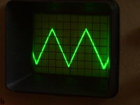
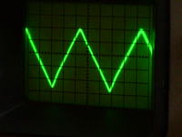
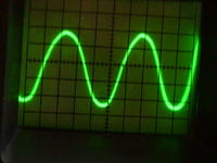
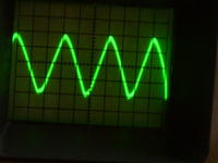
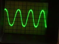
Photo 1 – 100kHz, 2,3 – 1MHz, 4,5 – 3MHz.
Link to original thread – Lifting generatora funkcyjnego
