anh56789
Junior Member level 1

Hi everyone,
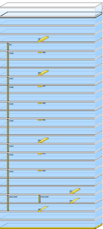
I'm working with 65nm CMOS technology and using the EM simulator from ADS software. I have attached a part of the EM substrate stack-up, and I have some questions about the bottom cover.
I'm working with 65nm CMOS technology and using the EM simulator from ADS software. I have attached a part of the EM substrate stack-up, and I have some questions about the bottom cover.
- I was told that the perfect conductor at the bottom is used as a reference pin for every port in the EM simulation, except for differential ports. In GaN or GaAs technology, there is a backside metal, which I assumed the bottom cover also represented. However, in CMOS technology, there isn’t any metal beneath the final layer, which is the silicon substrate. How might this affect the validity of the EM simulation results?
- After simulating the CMOS circuit, I generated an SNP file for circuit simulation and noticed that there is a reference pin for the bottom cover. I’m curious about the purpose of this pin, especially considering that the CMOS chip is placed on the center ground pad of the package with adhesive, leading to a connection from the bottom cover to the ground with finite impedance. What should we do regarding this pin when packaging the chip? Furthermore, I found that when simulating the SNP file with the reference pin connected to ground versus floating, the results differ.


