Continue to Site

Welcome to EDAboard.com

Welcome to our site! EDAboard.com is an international Electronics Discussion Forum focused on EDA software, circuits, schematics, books, theory, papers, asic, pld, 8051, DSP, Network, RF, Analog Design, PCB, Service Manuals... and a whole lot more! To participate you need to register. Registration is free. Click here to register now.

Reason of measurements of Cap 1812 footprint

Status
Not open for further replies.

CataM

Advanced Member level 4
Joined
Dec 23, 2015
Messages
1,275
Helped
314
Reputation
628
Reaction score
312
Trophy points
83
Location
Madrid, Spain
Activity points
8,409
Hello everyone,

Here is a 1812 (4532 metric) SMD Cap: https://www.digikey.es/products/es?keywords=445-1607-1-ND

If one goes to the footprint provided by UltraLibrarian as follows: DigiKey link --> Download from UltraLibrarian --> Detailed view in the Footprint, we see the following:
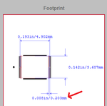
C1812.png

Pointed with the arrow shows that half of the pad=0.203mm

According to IPC-7531, the pad should be 1.6mm (maximum) or 1.2mm (minimum).

Can anyone provide me the reason why UltraLibrarian is using a lot less of pad width ? Are they mistaken ?
 

Are you sure you have attached the correct snapshot ?
The picture is from an IC, but the link refers to an SMD capacitor.
 

Yes, I have attached DigiKey link and instructions to get to that information. You can check it. It is correct and very weird !
 

Ops, my fault, you are correct.
There is a big error in the size.
 

There is a big error in the size.
O.K. So it is an error.

I don't want to provide the altium files because you would say I have corrupted the file. I want you you guys to check it.

Here is step by step:
From DigiKey link --> Click on "Download from UltraLibrarian" --> follow this video

What you get in Altium footprint is exactly what you see on the "Detailed view" on the Footprint from UltraLibrarian, like here:
link.png
 

It is not clear by whom the models available on the Ultralibrarian are made (is it from colaborative repository among manufacturers? are made by Digikey staff itself?). So far I have had no problems with even more complex ICs, but maybe it is time to review the feasibility of this site as a trustable source of footprint models.

- - - Updated - - -

BTW, I have used this site to get my Altium models, even reaching the monthly quote.
I've used exactly the same process described in the video.
 

It has been stated on several occasions, get familiar with IPC-7351.

I am a professional PCB designer for over 30 years now and i never download footprints from the internet. Learn the IPC-7351 standard and create your footprints
accordingly. I know it is tempting to download them and may be OK for hobby projects, but thats it. (imho)
 
  • Like
Reactions: CataM

    CataM

    Points: 2
    Helpful Answer Positive Rating
Status
Not open for further replies.

Part and Inventory Search

Welcome to EDABoard.com

Sponsor

Back
Top