Continue to Site

Rdson of a GaN FET

HariHerekar

Newbie level 6
Newbie level 6
Joined
Aug 19, 2024
Messages
14
Helped
0
Reputation
0
Reaction score
0
Trophy points
1
Activity points
143
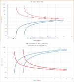
Hey all, just wanted clearing up on this concept. I have a range of VDS vs IDS values I obtained by testing the device GS66508B on a Keysight curve tracer.
To find its RDSON, is it as simple as VDS/IDS ? I know that values must be in the linear region where VGS-Vth>VDS, but are there any extra parameters i must keep in mind while finding the RDSON for a GaN FET ?
Also, i know the equivalent circuit for the small signal behaviour in the saturation region is a voltage dep. current source, but is this behavior valid for large signals as well ?
If so, is VDS/IDS in saturation also an RDSON ?
 
Ids = 0.5β(Vgs - Vgs(th))² for saturation

revised.... sigh

Use datasheet only Rds= Vds/Id [Ω]

In order to see the entire range look at the "nominal" plots but only tables are guaranteed.


ON is the tested RdsOn in the tables @ Vgs, Tj. Ids and Tj max using constant current = 9A

Heat will raise RdsOn with temperature ~250% with a rise of 125'C to 150'C
also Id rises RdsOn rapidly above 50A,.


Take 2

The plots are rather non linear.

The pink slope is Vgs=Vds I used to define the saturation boundary.

1742331406723.png
 

Attachments

  • 1742326219056.png
    1742326219056.png
    124.7 KB · Views: 14
  • 1742328187277.png
    1742328187277.png
    466.4 KB · Views: 13
  • 1742331979565.png
    1742331979565.png
    234.3 KB · Views: 12
Last edited:
A FET meant for switching applications will rate at a
reasonable Vgs and a Vds "as if" it had switched
hard and is carrying relevant current. That's the job.

Sweeping Vds across 0 - BVdss is not for this. That
is for model pulls.

Here is the datasheet electrical table. See right there,
third row? Test conditions. Forget the temperature
or assert your own.

1742342053129.png
 
The Figures of Merit (FoM) for this part is it's RdsOn*Cout' at 400V or RdsOn*Qoss product. This results is shorter switching times.
The down side is the RdsOn is much higher than a Si chip of similar size, requires a negative Vgs to turn off faster and the tolerance for Vgs(th) max/min is 2.36. This variation comes the β=1/2⋅μ⋅Cox⋅W/L process control.
1742342797327.png


If you ignore the excessive Id max> 50 A for the GaN FET, here I attempted to set Vgs=Vds and short circuit current by computing Id, and Ron vs Vgs=Vds. But Rds increases above 50A is not accounted for and I had to compute the Beta from the rated RdsOn. It didn't turn out perfectly because Beta changes from Vgs(th) min to max and they do not specify RdsOn min to max.

1742342746337.png
 
Thank you all for your replies, and thank you Tony for going the extra step as always. I built a little simulation in ADS that allows me to impress a pulsed voltage [Width of 20usec] on the drain and therefore obtain VDS,IDS values. My intention with the question was to find out if these can be used to plot RDSON, and if so, which values accurately represent the RDSON. Ive attached what one pulse looks like, and i do get an RDSON of appx 50mohm. My issue is that when I ramp up the voltage, the RDSON will rightly increase as Tj increases and IDS decreases. In such a case I am limiting myself to IDS,VDS values in the linear range to find out the degraded RDSON.
 

Attachments

  • 1pulseEDA.png
    1pulseEDA.png
    36.1 KB · Views: 9


Write your reply...

LaTeX Commands Quick-Menu:

Part and Inventory Search

Welcome to EDABoard.com

Sponsor

Back
Top