R and C values for a bldc card
- Thread starter jmx66
- Start date
- Status
- Not open for further replies.

- Joined
- Jan 22, 2008
- Messages
- 53,701
- Helped
- 14,811
- Reputation
- 29,919
- Reaction score
- 14,439
- Trophy points
- 1,393
- Location
- Bochum, Germany
- Activity points
- 303,603
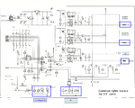
You mean the R and C connected through JP1? They set the output current limit and this way adjsut the PWM setpoint. The limit comparator has a threshold of about 100 mV, the sense resistor is shown with a 0.012 ohm value. So without a resistor connected to JP1, the current limit is set to about 8.3 A. Connecting R35 creates a 1:1 divider and doubles the current threshold. The capacitors are used to prevent current spikes to trigger the comparator.
jmx66
Member level 5

Hi FvM,
Thanks for your really fast reply - about less than 5 minutes after post !!!!! -, in fact, my query is about R6 to R11 with their capacitors.( see num-risation0003-modif-1-png )
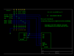
I draw a schematic - black scheme - and their labels are R1 -> R6 and C1 - > C6 .
And i don't know how to math R and C values...
Thanks a lot.
jm

- Joined
- Jan 22, 2008
- Messages
- 53,701
- Helped
- 14,811
- Reputation
- 29,919
- Reaction score
- 14,439
- Trophy points
- 1,393
- Location
- Bochum, Germany
- Activity points
- 303,603
Do you know the expected maximum output currents? As far as I understand, the current will be normally ruled by the PWM according to the speed setpoint. The current limit should only trigger in abnormal situations, e.g. a blocked motor. The capacitor dimensioning is discussed in datasheet Fig. 26. The actual current threshold is defined by 100 mV/0.012 ohm * (Rx+R35)/R35, where Rx is the resistor connected by JP1.
jmx66
Member level 5
Hi FvM,
Thanks a lot for your quick replies.
In fact , i 've just modified the original scheme , because i didn't ask question very clearly, with right scheme... Apologies.
So my query is about R6 to R11 and C11 to C16 see grey box with inside
" Values for R6 to R11
C11 to C16 "
Middle left side
I really read datasheet and AN, but with my mechanical background, didn't really how to math these values, hence my answer!!!!!
Thanks a lot.
jm
Ps: Now going to bed, tomorrow five o' clock in the morning.....
Attachments
- Joined
- Jan 22, 2008
- Messages
- 53,701
- Helped
- 14,811
- Reputation
- 29,919
- Reaction score
- 14,439
- Trophy points
- 1,393
- Location
- Bochum, Germany
- Activity points
- 303,603
O.K., I didn't notice this additional point. That's more easy. The resistors are simply pull-ups to be used with input switches and the open collector hall-effect sensor outputs. There are already pull-ups inside the IC (20k and 40k according to the datasheet). I would e.g. place 10 k for each external resistors, and a capacitor around 1 nF to filter possible spikes. But I'm not sure, if they are needed. You should also check the halls sensor specification for the specified ouput load.
- Status
- Not open for further replies.
Similar threads
-
How can I implement a BLDC motor to replace a 1 HP motor currently running a pump?
- Started by thannara123
- Replies: 3
-
-
Need to design and build 250W BLDC inverters for drones.
- Started by cupoftea
- Replies: 4
-
-


