Continue to Site

Welcome to EDAboard.com

Welcome to our site! EDAboard.com is an international Electronics Discussion Forum focused on EDA software, circuits, schematics, books, theory, papers, asic, pld, 8051, DSP, Network, RF, Analog Design, PCB, Service Manuals... and a whole lot more! To participate you need to register. Registration is free. Click here to register now.

[SOLVED] Quite Weird One: OffGridShapeError After Drawing The Path in Diagonal Snapping

Status
Not open for further replies.

powerofthedream

Newbie level 6
Newbie level 6
Joined
May 3, 2013
Messages
13
Helped
0
Reputation
0
Reaction score
0
Trophy points
1,281
Activity points
1,415
Virtuoso Layout Off-Grid-Shape Error, After Drawing The Metal Path in Diagonal Snap

Hey friends,

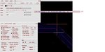
No 45 degree shape is allowed in some process, but my question is, why the inductor from the standard library has the 45-degree angles? How could the foundry manage that if it can NOT allow the designer to have polygon shapes ? Thanks so much for your enlightenments !
 

Attachments

  • Layout issue0618.jpeg
    Layout issue0618.jpeg
    113.9 KB · Views: 132
Last edited:

For standard library inductors exceptional rules re. 45° shapes are applied (because for such devices a 45° layout is more important than the unwanted database inflation due to 45° angles). The exception rule is laid down somewhere in the inductors' properties. Perhaps you could find this in your PDK's docu.
 
Often you'll see a non-printable "marker" layer which will
suppress (or enable) certain rule sets; "inductor" might
key some special extract and drc rules for this element,
while "esd" might enforce pullbacks and additional guard
structures and spacings, etc.

Just because some document or CAD guy says it's the law,
doesn't mean there's not a corresponding loophole.
 
Hey guys, thanks for your great knowledge to share, really terrific, have a good day!
 

Status
Not open for further replies.

Part and Inventory Search

Welcome to EDABoard.com

Sponsor

Back
Top