Alan8947
Full Member level 4

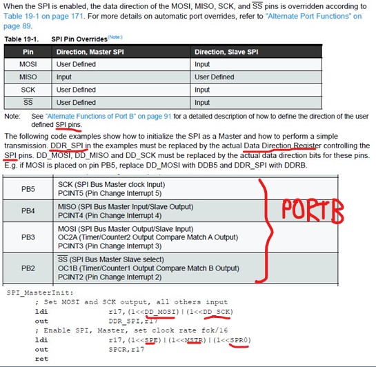
I have questions and verification of the coding. Here is a copy of the relevant part from the datasheet of page 170 and 91.

1) Is DDR_SPI just a given name of Data Direction Reg DDRB with address 0x04(0x24) in p100? Just to make it easier to understand the program. There is NO real DDR_SPI register.
2)From DDRB for PortB shown, MOSI is bit3, SCK is bit5. Therefore in line 2 of code above, DD_MOSI = 3, DD_SCK=5.
meaning (1<<DD_MOSI)=0b00001000, (1<<DD_SCK)=0b00100000, AND (1<<DD_MOSI) | (1<<DD_SCK) = 0b00101000 in binary. is this correct?
3) If (2) above is correct, why do all the shifting? That waste a lot of time clocking and slow down the program. why can't I just write like this:
DD_MOSI = 0b00001000
DD_SCK = 0b00101000
ldi r17,(DD_MOSI) | (DD_SCK) ; Loading 0b00101000 into r17, same as with the shifting by save a lot of time.
I know I am wasting my time on this, BUT I just want to go deeper. I might be wrong, but I feel I learn more if I do this than just take a short cut go directly to C++ and use other people's sub routine.
thanks

