wang wang
Newbie

The textbook mentions that when drawing a layout, attention must be paid to current density. Insufficient metal width may potentially lead to burnout, resulting in an open circuit.
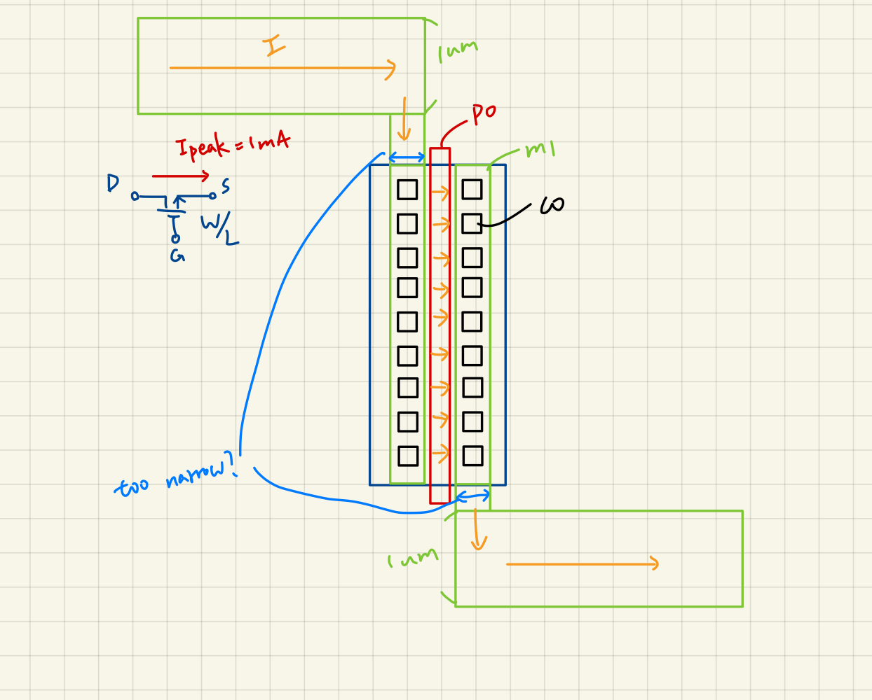
When I use the 'i' command to create an NMOS, it defaults to utilizing the minimize rule, generating a layout resembling the one in the image. Assuming I already know the maximum current flowing through this NMOS is 1mA and the current density for M1 is 1mA/1um, I have opted for a 1um width for the M1 connection. However, the connection region is still too narrow. Is this approach acceptable, or should I employ the finger technique by parallel connecting multiple drain terminals?

When I use the 'i' command to create an NMOS, it defaults to utilizing the minimize rule, generating a layout resembling the one in the image. Assuming I already know the maximum current flowing through this NMOS is 1mA and the current density for M1 is 1mA/1um, I have opted for a 1um width for the M1 connection. However, the connection region is still too narrow. Is this approach acceptable, or should I employ the finger technique by parallel connecting multiple drain terminals?