Continue to Site

Welcome to EDAboard.com

Welcome to our site! EDAboard.com is an international Electronics Discussion Forum focused on EDA software, circuits, schematics, books, theory, papers, asic, pld, 8051, DSP, Network, RF, Analog Design, PCB, Service Manuals... and a whole lot more! To participate you need to register. Registration is free. Click here to register now.

pulse current divider question

yefj

Advanced Member level 5
Joined
Sep 12, 2019
Messages
1,505
Helped
1
Reputation
2
Reaction score
5
Trophy points
38
Activity points
9,114
Hello, generally when i design an RF power divider its always about the impedance of the lines(Suppuse its T-junction).i do a champers and formulas to get a good insertion loss and return loss.
my line width is always an impedance calculation.
Here i have a different kind of situation. I have a demand to deliver 3A and 6V to a drain for 5 devices from a single source.
my pulse is 50u with 35% duty cycle and 20nsec rise and fall time

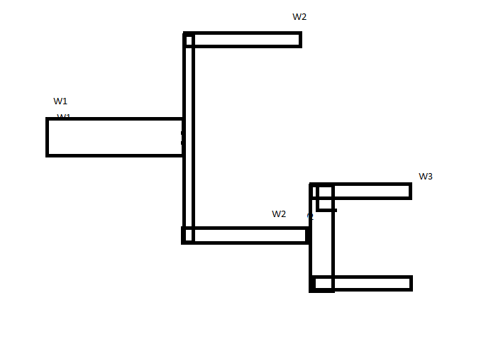
Using formulas i have found w1 w2 w3 :
W1=100mil 13 degree rise for 15A
W2=40mil 12.6 degree rise for 7.5A
etc..
I have the following problems:
1.my line width are not impedances but the width which could handle the current pulse.
How to construct the current divider for such case?
2.i need also need to deliver the square pulse intact, how do i consider the delivering the spectral data safely to the destination?
3.given my signal pulse how do i know what bandwidth to consider as containing most of its spectral pulse data?
4.I have SMA connector of 50 Ohms delivering this pulse,so once again how do i match the 50Ohm connector to the main artery trace which has to be 100mils just so it could wistand the current. 100 mils is not 50 Ohms to the signal.
Thanks.
1701534629461.png
 
Last edited:
Maybe start with parsing the requirement. That is, is "deliver" to mean
that the current -to- the drain is regulated, or that the current is
-allowed- if the FET and load want it?

I think that you are overthinking the problem with all this "RF stuff"
when you're talking 20ns risetimes (in my "gut" take, call 20ns a
quarter cycle of fundamental sine wave, give or take - so 12MHz),
that's not worthy of such fine impedance figuring and just wants
fat traces that can take the current at the duty cycle.

Of course for waveshape qualities you want some harmonics but
even with the 7th in play, you're still below 100MHz.

But I'm no RF expert. I just don't see this as a RF problem. And I
think that current control is either tail-bias or load-determined if
you just make the traces fat enough for the current.
 
Hello dick_freebird, ok so my spectral data is till 200Mhz.
I will do as you said and do a current deliver like in a tree shown above?
Then i will simulate it in EM simulator and see the S-param.
my voltage stays 6 V all the way ,my current goes from 15A to 3A at the destination.
What kind of S-params to expect to see that the current divider works good divides the current from 15A to 3A?
Thanks.
 
Having read your previous posts, we know that the question is again related to QPA2575 pulsed power supply.

According to QPA2575 datsheet, the expected power supply is a pulsed voltage source. The terms power divider or current divider seem inappropriate for the problem in my view, also no impedance matching is primarily involved. Nevertheless trace impedances have to be considered when designing the network.
 
Hello FVM,why its innapropriate the pulse of 6V on the drain creates a 3A drain current (as shown below)on each amplifier from each 6V pulse.
So we delivering 3A to each amplfier and 15A is the total current.
Why my logic is wrong?

1701540024818.png
 
Obviously amplifier supply currents are summing to total supply current. But what's the significance of calling it a current divider?

According to usual circuit math, 20 ns rise/fall time corresponds to 18 MHz bandwidth. Traces below 1/10 wavelength (about 40 cm length) can be analyzed as lumped parasitic elements, in this case primarily series inductance.
 
Hello dick_freebird, ok so my spectral data is till 200Mhz.
I will do as you said and do a current deliver like in a tree shown above?
Then i will simulate it in EM simulator and see the S-param.
my voltage stays 6 V all the way ,my current goes from 15A to 3A at the destination.
What kind of S-params to expect to see that the current divider works good divides the current from 15A to 3A?
Thanks.

I would try to model interconnect parasitics and do everything in the time
domain. Everything you mention about input and output seems to be DC
or transient pulse. Why the roundabout approach? S-params won't show
you voltage and current flat-top and only hint at ringing / settling time.
It's a pulse according to everything shown so far, so treat it as one?

There's also that the active device's own S-params may be, likely are,
different at resting bias and pulse bias.
 
Last edited:
Switch design might be the more demanding part of the design. PCB wiring can be modelled by series resistance and inductance in the first order. As for load characteristic, I/V diagram in post #5 suggests that load differential resistance is higher than 6V/3A. To simulate 0 -> 6 V and 6 -> 0 V transition correctly, we should have a large signal device model. I wonder also, if amplifier supply is pulsed with or without applied RF input. Current waveform will be respectively different.
 

LaTeX Commands Quick-Menu:

Part and Inventory Search

Welcome to EDABoard.com

Sponsor

Back
Top