Continue to Site

Welcome to EDAboard.com

Welcome to our site! EDAboard.com is an international Electronics Discussion Forum focused on EDA software, circuits, schematics, books, theory, papers, asic, pld, 8051, DSP, Network, RF, Analog Design, PCB, Service Manuals... and a whole lot more! To participate you need to register. Registration is free. Click here to register now.

Pspice Error - "Less than 2 connections at node"

Status
Not open for further replies.

Liz_S

Newbie level 3
Newbie level 3
Joined
Jan 12, 2018
Messages
3
Helped
0
Reputation
0
Reaction score
0
Trophy points
1
Activity points
29
Hello!
I tried to build this circuit:
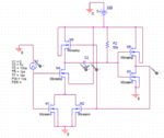
1.PNG

And I got this error:
*Analysis directives:
.TRAN 0 500ns 0
.OPTIONS ADVCONV
.PROBE64 V(alias(*)) I(alias(*)) W(alias(*)) D(alias(*)) NOISE(alias(*))
.INC "..\SCHEMATIC1.net"


**** INCLUDING SCHEMATIC1.net ****
* source WET3
X_U2 N00164 N00168 $G_DPWR $G_DGND INV
C_C1 N00160 N00164 2pF TC=0,0
R_R1 N00164 N00495 50k TC=0,0
X_U3 N00216 N00168 N00160 $G_DPWR $G_DGND NOR2
M_M1 N00744 N01953 0 0 Mbreakn
M_M2 N00744 N01801 0 0 Mbreakn
M_M3 N01801 N00857 0 0 Mbreakn
M_M4 N01046 N01953 N00744 N01357 Mbreakp
M_M5 N01357 N01801 N01046 N01357 Mbreakp
M_M6 N01357 N00857 N01801 N01357 Mbreakp
V_Vdd 0 N01357 5v
C_C2 N01046 N00857 2pF TC=0,0
V_V1 0 N01953
+PULSE 0 5v 10ns 1ps 1ps 1ns
R_R2 N00857 N01357 50k TC=0,0

**** RESUMING sim1.cir ****
.END


**** Generated AtoD and DtoA Interfaces ****

*
* Analog/Digital interface for node N00160
*
* Moving X_U3.U1:OUT1 from analog node N00160 to new digital node N00160$DtoA
X$N00160_DtoA1
+ N00160$DtoA
+ N00160
+ $G_DPWR
+ $G_DGND
+ DtoAdefault
+ PARAMS: DRVH= 50 DRVL= 50 CAPACITANCE= 0
*
* Analog/Digital interface for node N00164
*
* Moving X_U2.U1:IN1 from analog node N00164 to new digital node N00164$AtoD
X$N00164_AtoD1
+ N00164
+ N00164$AtoD
+ $G_DPWR
+ $G_DGND
+ AtoDdefault
+ PARAMS: CAPACITANCE= 0
*
* Analog/Digital interface power supply subcircuits
*
X$DIGIFPWR 0 DIGIFPWR


ERROR(ORPSIM-15141): Less than 2 connections at node N00495.

Thank you very much! Liz
 

The above Log mentions a resistor R1 that at first glance I could not see in the circuit. In fact, this resistor is connected to two other devices also not visible in the snapshot, namelly C1 and U2. Try zooming out to see what else is on the project sheet.
 
  • Like
Reactions: Liz_S

    Liz_S

    Points: 2
    Helpful Answer Positive Rating
The above Log mentions a resistor R1 that at first glance I could not see in the circuit. In fact, this resistor is connected to two other devices also not visible in the snapshot, namelly C1 and U2. Try zooming out to see what else is on the project sheet.

Thank you very much! I'm new to PSpice so I make silly mistakes, I apologize.

Now, for the same circuit, I'm running transient analysis and I get the following error:
ERROR(ORPSIM-15659): Discontinuing simulation due to convergence problem

I tried to solve it using methods I found online, and nothing helps...
 

Guess you want to move C2 connection to the NAND output (M1/M2/M4 drain).
 

PSpice Error - Convergence Problem

Hello!
I tried to build this circuit:


And I got this error:
1.PNG

Code:
*Analysis directives: 
.TRAN  0 500n 0 
.OPTIONS ADVCONV
.PROBE64 V(alias(*)) I(alias(*)) W(alias(*)) D(alias(*)) NOISE(alias(*)) 
.INC "..\SCHEMATIC1.net" 


**** INCLUDING SCHEMATIC1.net ****
* source WET3
V_Vdd         0 N05008 5v
M_M1         N04963 N05022 0 0 Mbreakn1           
M_M2         N04963 N05022 N05004 N05008 Mbreakp3           
M_M3         N04963 N05234 0 0 Mbreakn2           
M_M4         N05004 N05234 N05008 N05008 Mbreakp4           
C_C1         N04963 N05238  2p  TC=0,0 
M_M6         N05234 N05238 0 0 Mbreakn5           
M_M5         N05234 N05238 N05008 N05008 Mbreakp6           
R_R1         N05238 N05008  50k TC=0,0 
V_V1         N05022 0  
+PULSE 0v 5v 10n 1p 1p 1n 

**** RESUMING sim1.cir ****
.END

**** 01/13/18 13:20:38 ******* PSpice Lite (March 2016) ******* ID# 10813 ****

 ** Profile: "SCHEMATIC1-sim1"  [ C:\Cadence\SPB_17.2\wet3-pspicefiles\schematic1\sim1.sim ] 


 ****     MOSFET MODEL PARAMETERS


******************************************************************************


               Mbreakn1        Mbreakp3        Mbreakn2        Mbreakp4        
               NMOS            PMOS            NMOS            PMOS            
       LEVEL    1               1               1               1            
           L    3.000000E-06    3.000000E-06    3.000000E-06    3.000000E-06 
           W    3.000000E-06   12.000000E-06    3.000000E-06   12.000000E-06 
         VTO    2              -2               2              -2            
          KP  207.100000E-06  103.500000E-06  207.100000E-06  103.500000E-06 
       GAMMA    0               0               0               0            
         PHI     .6              .6              .6              .6          
      LAMBDA     .02             .02             .02             .02         
          IS   10.000000E-15   10.000000E-15   10.000000E-15   10.000000E-15 
          JS    0               0               0               0            
          PB     .8              .8              .8              .8          
        PBSW     .8              .8              .8              .8          
          CJ    0               0               0               0            
        CJSW    0               0               0               0            
        CGSO    0               0               0               0            
        CGDO    0               0               0               0            
        CGBO    0               0               0               0            
         TOX   10.000000E-09   10.000000E-09   10.000000E-09   10.000000E-09 
          XJ    0               0               0               0            
          UO                  300                             300            
       UCRIT   10.000000E+03   10.000000E+03   10.000000E+03   10.000000E+03 
      DIOMOD    1               1               1               1            
         VFB    0               0               0               0            
        LETA    0               0               0               0            
        WETA    0               0               0               0            
          U0    0               0               0               0            
        TEMP    0               0               0               0            
         VDD    5               5               5               5            
       XPART    0               0               0               0            


               Mbreakn5        Mbreakp6        
               NMOS            PMOS            
       LEVEL    1               1            
           L    3.000000E-06    3.000000E-06 
           W    3.000000E-06    6.000000E-06 
         VTO    2              -2            
          KP  207.100000E-06  103.500000E-06 
       GAMMA    0               0            
         PHI     .6              .6          
      LAMBDA     .02             .02         
          IS   10.000000E-15   10.000000E-15 
          JS    0               0            
          PB     .8              .8          
        PBSW     .8              .8          
          CJ    0               0            
        CJSW    0               0            
        CGSO    0               0            
        CGDO    0               0            
        CGBO    0               0            
         TOX   10.000000E-09   10.000000E-09 
          XJ    0               0            
          UO                  300            
       UCRIT   10.000000E+03   10.000000E+03 
      DIOMOD    1               1            
         VFB    0               0            
        LETA    0               0            
        WETA    0               0            
          U0    0               0            
        TEMP    0               0            
         VDD    5               5            
       XPART    0               0            


Starting pseudo-transient algorithm.

ERROR -- Convergence problem in transient bias point calculation


  Last node voltages tried were:

 NODE   VOLTAGE     NODE   VOLTAGE     NODE   VOLTAGE     NODE   VOLTAGE


(N04963)   -1.3975 (N05004)   -2.8130 (N05008)   -2.8130 (N05022)    0.0000     

(N05234)   -1.4065 (N05238)   -2.3899 


  These voltages failed to converge:

    V(N04963)                 =    -1.821V  \    -1.398V
    V(N05004)                 =    -2.809V  \    -2.813V
    V(N05238)                 =    -2.813V  \    -2.390V

  These supply currents failed to converge:

    I(V_Vdd)                  =   118.46pA  \   -10.00GA
    I(V_V1)                   =         0A  \   -1.036uA

  These devices failed to converge:
    M_M1      M_M2      M_M3      M_M6      M_M5      

ERROR(ORPSIM-15659): Discontinuing simulation due to convergence problem

**** Interrupt ****
Thank you very much! Liz
 

Re: PSpice Error - Convergence Problem

ERROR(ORPSIM-15659): Discontinuing simulation due to convergence problem

If you do a web search with the keywords "spice-convergence-workaround", you will find some common recommendations to adjust the simulation parameters in order to eliminate this error, but another alternative that often solves this is to perform the simulation, not with ideal components, but with real components (which in other words are modeled with parasitic elements). I'm not familiar with the PSPICE libraries, but at least in LTSPICE there are models of many 'real' devices. Another possibility is to place some components in the above circuit which do not impact on it performance, but prevents computing from being trapped around an oscillating state not steady (this so-called "convergence error" condition), such as adding high value pull-up/pull-down resistors in parallel to nodes to assert expected default values, as well as adding small value resistors in series to nodes where should not have infinite current, for example between each MOSFET totem. All these extra components would help the circuit to act as the real world behaving, for example, the current limiting due to wiring, as well as having asymmetry in biasing that forces the floating nodes to a random or determined state.
 

Status
Not open for further replies.

Part and Inventory Search

Welcome to EDABoard.com

Sponsor

Back
Top