Continue to Site

Welcome to EDAboard.com

Welcome to our site! EDAboard.com is an international Electronics Discussion Forum focused on EDA software, circuits, schematics, books, theory, papers, asic, pld, 8051, DSP, Network, RF, Analog Design, PCB, Service Manuals... and a whole lot more! To participate you need to register. Registration is free. Click here to register now.

PS_MIO_VREF_501 signal in ZYNQ why connected to VREF0V9

Status
Not open for further replies.

engr_joni_ee

Advanced Member level 3
Joined
Nov 3, 2018
Messages
822
Helped
2
Reputation
4
Reaction score
7
Trophy points
18
Activity points
6,878
Hi,

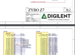
I have attached PS MIO Bank schematic of ZYBO development board. The MIO Bank 501 is powered up by 1.8 V and MIO Bank 500 is powered up by 3.3 V.

I am wondering why the signal PS_MIO_VREF_501 in MIO Bank 501 is connected to VREF0V9 ? and why not connected to GND ? What about if we leave it un-connected in the new board ?
 

Attachments

  • Untitled.png
    Untitled.png
    198.9 KB · Views: 172

You want to read the ZYBO-Z7 reference manual...

The Zynq incorporates two independent Gigabit Ethernet Controllers. They implement a 10/100/1000 half/full duplex Ethernet MAC. Of these two, GEM 0 can be mapped to the MIO pins where the PHY interfaces. Since the MIO bank is powered from 1.8V, the RGMII interface uses 1.8V HSTL Class 1 drivers. For this I/O standard an external reference of 0.9V is provided in bank 501 (PS_MIO_VREF). Mapping out the correct pins and configuring the interface is handled by the Zybo Z7 Vivado board files.
 
Status
Not open for further replies.

Part and Inventory Search

Welcome to EDABoard.com

Sponsor

Back
Top