Continue to Site

Welcome to EDAboard.com

Welcome to our site! EDAboard.com is an international Electronics Discussion Forum focused on EDA software, circuits, schematics, books, theory, papers, asic, pld, 8051, DSP, Network, RF, Analog Design, PCB, Service Manuals... and a whole lot more! To participate you need to register. Registration is free. Click here to register now.

Problems with my ESD protection circuit

Status
Not open for further replies.

mmteogangco

Newbie level 2
Newbie level 2
Joined
Aug 5, 2010
Messages
2
Helped
0
Reputation
0
Reaction score
0
Trophy points
1,281
Location
Philippines
Visit site
Activity points
1,298
ESD RC Trigger

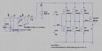
Hi! Can somebody help me. I cant seem to know the problem with my ESD protection circuit.

The voltage at the capacitor (C4) of the RC trigger dont change even with ESD events, so causes an open power clamp at all times. I hope to know the problem.

:cry: Ciel


ESD RC Trigger

To begin with, returning the ESD source to gnd! is not very realistic.
It should return to one or the other rail (VDD, VSS) through a
replica pin protection diode network, unless you are only trying
to test one, less challenging case. Pin to pin, not pin to ideal return.

Now plot VDD, VSS and their difference voltage, and the R1/C4
voltage. That should tell you all you need about the trigger waveform
you have to work with.

Consider that many integrated capacitors have a lot of parasitic
loss and charge division results, which takes away from
trigger robustness. And your trigger needs also to pass through
the protection diodes into the rails without much loss as well.

Your ESD trigger circuit looks kind of kooky to me. Maybe you
want to also step back and apply a more traditional HBM source
model. I see no reason why you would get a useful (certainly
not realistic) output from what you've got.

Finally, you have a stiff 5V VDD, -5V VSS due to the sources
and no pulse out of the "stinger" will perturb them. ESD is an
unpowered threat phenomenon for the most part and the
clamp scheme you show is meant for unpowered operation
(depending on the supply rails to slew, hard, for triggering).
If you are trying to test some powered ("line ESD") scenario
you need a different scheme. If you are testing traditional ESD
(loose part) then you need the supply pins open circuit.
 

Re: ESD RC Trigger

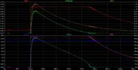
thanks for the reply. I made some revisions, just like what you said and also I considered suggestions from esd experts.

I got an output, just want to check if this is right?

I have also a few questions in mind, like:

1. Why does the input voltage of the 1st inverter V(invi) does not change but the output changes(Vinvo)? Is it beacuse of the current at R1 (IR1)?

2. Is the power clamp current (Iclamp) enough, to protect the VDD source?

3. How can I improve the output waveform (clamp)?

Thanks for the help. I got more excited after I saw the results. :D


Re: ESD RC Trigger

From my experience, the RC value is too large, you can try to decrease the RC value, see the difference.
 
Last edited:

Re: ESD RC Trigger

from your 1st schematic, it seems that the pusle(0 2000 10n 1n 10n 1n ) has some problem? what is the pusle width and period? and you are charging the 100pF cap while discharging at the same time, you should use a switch like the later schematic you post, close the switch after the 100pF cap is completed charged.

from the later schematic, you added a VDD=5V at the power rail, actually HBM happens at human handling and transportation, but seldom at chip normal operation. so i think you can forget about the power supply while you are simulating HBM.

as xiangxianga396 said, the time constant you set is 10K*10u=100ms, which is too large! even the former one 50K*20p=1us a little bit large, you can set at about 0.1us or so, the voltage can be easily coupled and driven to low (for former one with PMOS) or high (for later one NMOS) at the gate of the main ESD discharging MOSFET due to serveral stages of inverters you have added.

---------- Post added at 14:38 ---------- Previous post was at 14:31 ----------

i am trying to answer your questions:

Q1. Why does the input voltage of the 1st inverter V(invi) does not change but the output changes(Vinvo)? Is it beacuse of the current at R1 (IR1)?
A: V(invi) is forced by the VDD=5V your added at the power rail through the large resistor R1=10K.

Q2. Is the power clamp current (Iclamp) enough, to protect the VDD source?
A: the current is enough, also you should check the clamping voltage, but it seems that you have to remove the VDD=5V.

Q3. How can I improve the output waveform (clamp)?
A: re-size the RC time constant.
 

Re: ESD RC Trigger

The C value is unrealistically large for an IC. However you need
the time constant to be very large, in order that the ESD source
energy will be fully dissipated before the clamp releases. If you
do not ride out the source time constant, to many tau (how many,
to get (say) down to 3V/2000V at the source cap?) you will be
dissipating the remaining energy in an untriggered shunt or the
core circuitry. Or you will "motorboat" in and out of clamp at the
release-rate of the trigger.

Your opposite constraint is that you must not trigger on the
fastest allowed input supply risetime under (worst-)normal
application conditions (or specify a user constraint, which is
not especially popular).
 

Status
Not open for further replies.

Part and Inventory Search

Welcome to EDABoard.com

Sponsor

Back
Top