Continue to Site

Welcome to EDAboard.com

Welcome to our site! EDAboard.com is an international Electronics Discussion Forum focused on EDA software, circuits, schematics, books, theory, papers, asic, pld, 8051, DSP, Network, RF, Analog Design, PCB, Service Manuals... and a whole lot more! To participate you need to register. Registration is free. Click here to register now.

Problems choosing capacitor and resistor value for LM 2917

Status
Not open for further replies.

nsypid

Junior Member level 3
Joined
Dec 21, 2011
Messages
25
Helped
0
Reputation
0
Reaction score
0
Trophy points
1,281
Activity points
1,442
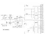
The datasheet states that Vo= VccxfinxC1xR1.
I want to know what is the value of Vcc in my attached circuit diagram.

and also Fmax = I2/C1xVcc
What is the value of I2 here ?

What value of R1, C1 and C2 should i use if i want to measure up to 250 Hz input signal with that circuit ?
 

Attachments

  • ledtachot3.jpg
    ledtachot3.jpg
    92.6 KB · Views: 179

The LM2917 has an internal 7.5V zener diode between the power supply input (pin No.9) and ground and that's the Vcc value that should be used for calculations. In the circuit you linked to, the 12V supply is first down-regulated to 9V by the 7809. The 9V is fed to the internal zener diode via R4 (470 0hms).

Regarding your other questions, I've used the LM2907 (without an internal zener diode) in a few designs, but that was years ago and I'm a bit rusty about some details of its characteristics. I don't have time to check the datasheet right now. I'll be back later if no one else has given you the answers you need by then.
 
  • Like
Reactions: nsypid

    nsypid

    Points: 2
    Helpful Answer Positive Rating
I2 is the charge pump current through pin No.2 which is given on the datasheet as about 165uA at Vcc of 7.5V.

For the circuit you're considering, matching the output voltage to the display input sensitivity at the maximum frequency you want to display is more important than the max possible input frequency. What that means is this:

The full-scale input of each LM3914 is 1.25V. Since two LM3914s are cascaded here, the input for full-scale display is 2.5V. Therefore, if you want the display to show full scale at 250Hz, the LM2917's output should be 2.5V at 250Hz. Taking the formula given on the datasheet -

Vo = Vcc*fin*C1*R1 or, if we use the part Nos. in the circuit you uploaded: Vo = Vcc*fin*C6*R5
This can be arranged as C6*R5 = Vo/(Vcc*Fin)
Since Vcc = 7.5V, fin is 250Hz max, Vo = 2.5V at 250Hz
Then C6*R5 = 2.5/1875 = 0.00133
If we use the value of C6 already given as 47nF or 0.047uF
Then R5 = 0.00133/0.047 = 0.0283. This calculated value of R5 is in Megohms since C6 was given in uF
Therefore R5 = 28.3k which is within the adjustment range for the 50k pot
In practice, it is best to put a fixed resistor of 10-15k in series with the 50k pot.

Using the values of I2 = 165uA and Vcc = 7.5V
fmax = 468 Hz. This result assures us that the IC will still be operating in the linear region at 250Hz.
But the output voltage Vo at fmax is about 4.68V which is well above the full-scale input of the display section. We've already calculated the component values to give full-scale display at 250Hz. Therefore any input frequency above 250Hz will make no difference in the display.
 
  • Like
Reactions: nsypid

    nsypid

    Points: 2
    Helpful Answer Positive Rating
Thanks.

There is still some part in the circuit diagram which i don't understand.
The signal that i am measuring is 12v pulse. What is the function of C1,R1,C4,R2,DZ1 here ?
Is it ok if i exclude those components ?
 

C1 blocks DC.
R1 limits current through DZ1 and the LM2917 input in case of high input voltages. It also forms a high-frequency filter (low-pass) with C4.
C4 bypasses high-frequency spikes and interference.
R2 is the bias resistor for the LM2917 input transistor.
DZ1 protects the LM2917 input by clamping high voltage inputs to +12V and -0.6V
 
  • Like
Reactions: nsypid

    nsypid

    Points: 2
    Helpful Answer Positive Rating
Another question: When i simulate the circuit diagram in proteus, i get output signal from lm 2917 like in my attached picture. The input signal is yellow and the output signal is blue. What are my options to reduce ripple voltage on output signal ?
 

Attachments

  • Output lm 2917 rpm led.PNG
    Output lm 2917 rpm led.PNG
    76.8 KB · Views: 135

The amount of ripple is most directly affected by the size of C7. Increasing C7 (currently 2.2uF) will reduce ripple in direct proportion to its capacitance. However, the datasheet says that increasing C7 slows down response to changes in input frequency. The datasheet isn't clear about how the response time can be estimated. I guess the time constant R5*C7 would be valid as a starting point.

One thing you should consider is - By how much do you need to reduce the ripple? The oscillogram shows it as about 100-150mV p-p. The LM3914 has a resolution of 125mV so that increasing C7 to 4.7uF or 10uF should be OK. No matter how much you increase C7, there will always be some ripple content in the output. When the LM2917 output voltage is near a transition level (e.g. near 625mV) the ripple will cause the display to flicker between adjacent dots. This cannot be completely avoided unless complex additional circuits are added. In any case, I don't consider it to be particularly objectionable.

(On a side note: My internet connection has been acting up again for the past few hours. It took me several minutes to download your image. This kind of thing happens from time to time in this remote location and the situation sometimes persists for days.)
 
  • Like
Reactions: nsypid

    nsypid

    Points: 2
    Helpful Answer Positive Rating
Thanks for your help. I hope this project can be realized asap.

btw what remote location are you talking about ?
 

Thanks for your help. I hope this project can be realized asap.
You're welcome. Do let us know how things turn out.

btw what remote location are you talking about ?
Well, I don't want to be rude, but I'd rather not reveal my location at this time except to say that it's in the most isolated state in the least developed region of a developing country. The state is surrounded on three sides by even less developed neighbouring countries :smile:. Communication with the rest of the country is either by air from a single airport or by road on a single so-called highway. No railway because it's too hilly.
 

Now I am really curious about your location! hahahahaha
 

Status
Not open for further replies.

Similar threads

Part and Inventory Search

Welcome to EDABoard.com

Sponsor

Back
Top