Continue to Site

Welcome to EDAboard.com

Welcome to our site! EDAboard.com is an international Electronics Discussion Forum focused on EDA software, circuits, schematics, books, theory, papers, asic, pld, 8051, DSP, Network, RF, Analog Design, PCB, Service Manuals... and a whole lot more! To participate you need to register. Registration is free. Click here to register now.

Problem with Gerber output from PADS

Status
Not open for further replies.

moin.gadiwan27

Newbie level 2
Newbie level 2
Joined
May 24, 2012
Messages
2
Helped
0
Reputation
0
Reaction score
0
Trophy points
1,281
Activity points
1,294
Hi,
This is Moin here.
I have a schematics which is 1173.0mm length and width 18mm (tube light).
In PADS I have designed layout.
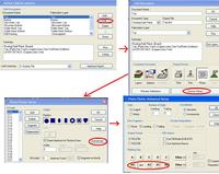
But generating Gerber is not possible as shown in the diagram 1,2,3.
Please help me in solving these issue.
 

Attachments

  • PADS 2.png
    PADS 2.png
    83.6 KB · Views: 98
  • PADS1.png
    PADS1.png
    76.9 KB · Views: 112
  • PADS3.png
    PADS3.png
    111.3 KB · Views: 99

But generating Gerber is not possible as shown in the diagram 1,2,3.
Diagram 3 suggests that you didn't setup correct gerber plot size, but nothing else is "shown".

However, before proceeding with the layout artwork, did you verify that your PCB manufacturer can produce the board size?
 

Can you tell me any other tool that meets my requirement.

- - - Updated - - -

Ya, manufactures can handle PCB..........

- - - Updated - - -

Hi,
Please help me out lib (PADS 9.0)
 

Hi,
file--->CAM-->select Top-->select Edit option-->Device setup -->then select advance-->change the plotting size

 
  • Like
Reactions: FvM

    FvM

    Points: 2
    Helpful Answer Positive Rating
You may have reached the physical limits of your design tool. You might try to move the origin (0.0) to the center of the board.
 

file--->CAM-->select Top-->select Edit option-->Device setup -->then select advance-->change the plotting size
You confirmed my assumption that Pads can plot larger gerber films, as every serious layout tool. A0 should be already sufficient, "OTHER" is probably allowing any plot size beyond the capabilities of your PCB manufacturer.
 

Status
Not open for further replies.

Part and Inventory Search

Welcome to EDABoard.com

Sponsor

Back
Top