problem with differential pair
- Thread starter ahmad1954
- Start date
- Status
- Not open for further replies.


Usama Siddiqui
Member level 5

did you made a proper mirror i.e all the same values of resistors and transistors ??


- Joined
- Oct 9, 2009
- Messages
- 10,865
- Helped
- 2,065
- Reputation
- 4,130
- Reaction score
- 1,597
- Trophy points
- 1,403
- Location
- Yorkshire, UK
- Activity points
- 57,270
Because you have fixed M2 gate and varied M1 gate. You have not applied a symmetric differential input signal.
Keith
Keith
ahmad1954
Full Member level 4
so what should I do for symmetric output? should I apply another source to M2 gate? in this case which source should vary for calculating linearity range?
- Joined
- Oct 9, 2009
- Messages
- 10,865
- Helped
- 2,065
- Reputation
- 4,130
- Reaction score
- 1,597
- Trophy points
- 1,403
- Location
- Yorkshire, UK
- Activity points
- 57,270
You should increase one input as you decrease the other so as one goes from 3V to -3V to other goes from -3V to +3V.
Keith
Keith
- Joined
- Oct 9, 2009
- Messages
- 10,865
- Helped
- 2,065
- Reputation
- 4,130
- Reaction score
- 1,597
- Trophy points
- 1,403
- Location
- Yorkshire, UK
- Activity points
- 57,270
ahmad1954
Full Member level 4
What software did you use?
I tried your idea in hspice and I received this error: **error** inductor/voltage source loop found containing 0:vdc1 defined in subckt 0
this is new code:
Vdc1 1 6 0
vcm 6 0 3
VCC 11 0 DC 5
VDD 12 0 DC -5
M1 3 1 5 5 NMOS1 w=10u l=.1u
M2 4 7 5 5 NMOS1 w=10u l=.1u
RC1 11 3 1k
RC2 11 4 1k
RE 5 12 7.2K
E1 1 6 6 7 1
.MODEL NMOS1 Nmos level=2
.print dc id(m1) id(m2)
.dc vdc1 -3000m 3000m 1m
- Joined
- Oct 9, 2009
- Messages
- 10,865
- Helped
- 2,065
- Reputation
- 4,130
- Reaction score
- 1,597
- Trophy points
- 1,403
- Location
- Yorkshire, UK
- Activity points
- 57,270
I think your E1 is incorrect. HSPICE has output nodes first then input nodes. Try E1 7 6 6 1 1
I use SIMetrix, but the simulator shouldn't matter - it should work any any SPICE simulator (with slight syntax differences).
Keith
I use SIMetrix, but the simulator shouldn't matter - it should work any any SPICE simulator (with slight syntax differences).
Keith
- Joined
- Oct 9, 2009
- Messages
- 10,865
- Helped
- 2,065
- Reputation
- 4,130
- Reaction score
- 1,597
- Trophy points
- 1,403
- Location
- Yorkshire, UK
- Activity points
- 57,270
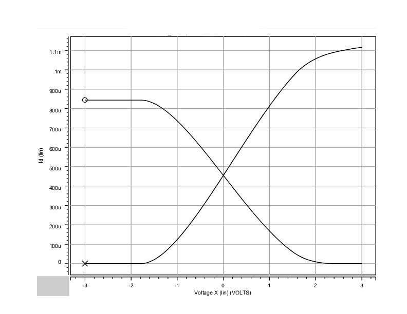
And hopefully symmetrical now.
Keith
Keith
ahmad1954
Full Member level 4
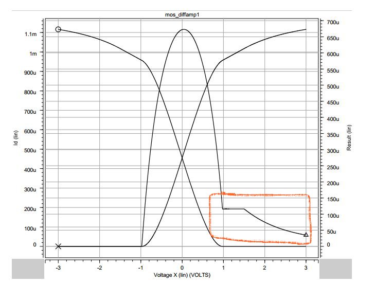
now I want to calculate GM. by definition I should calculate d(Iout). the output is shown below:

my question is why the red rectangle in the right of the figure is this form?
my question is why the red rectangle in the right of the figure is this form?
- Joined
- Oct 9, 2009
- Messages
- 10,865
- Helped
- 2,065
- Reputation
- 4,130
- Reaction score
- 1,597
- Trophy points
- 1,403
- Location
- Yorkshire, UK
- Activity points
- 57,270
It depends how you calculated it. The current drops to zero and you may have a divide by zero in there.
Keith
Keith
LvW
Advanced Member level 6
Hi ahmad1954,
just for a better understanding of the differential pair:
Your output characteristics would exhibit better symmetry - even if you apply one single input voltage only - if you reduce the common mode gain by increasing the common emitter resistance.
An ideal diff. pair has a current source in the emitter path (resistance approaching infinite) with a nearly ideal common mode rejection ratio and symmetrical output curves.
- Joined
- Oct 9, 2009
- Messages
- 10,865
- Helped
- 2,065
- Reputation
- 4,130
- Reaction score
- 1,597
- Trophy points
- 1,403
- Location
- Yorkshire, UK
- Activity points
- 57,270
What equation have you plotted to get gm? I am not sure it looks correct.
Keith
Keith
- Joined
- Oct 9, 2009
- Messages
- 10,865
- Helped
- 2,065
- Reputation
- 4,130
- Reaction score
- 1,597
- Trophy points
- 1,403
- Location
- Yorkshire, UK
- Activity points
- 57,270
For a differential pair I would have thought you would want diff(Id1-Id2)/diff(Vg1-Vg2) but it depends on what your objective is. Your syntax might be slightly different to mine (DERIV for HSPICE I think). I don't see any strange discontinuities doing that and the gm tails off rather than making an abrupt drop to zero which is what yours seems to do.
Keith.
Keith.
Attachments
- Status
- Not open for further replies.
Similar threads
-
-
-
Problem delay in switching current steering differential DAC
- Started by PhdSA
- Replies: 5
-
-
Glitch problem o differential transmission gate in cadence
- Started by PhdSA
- Replies: 8