Continue to Site

Welcome to EDAboard.com

Welcome to our site! EDAboard.com is an international Electronics Discussion Forum focused on EDA software, circuits, schematics, books, theory, papers, asic, pld, 8051, DSP, Network, RF, Analog Design, PCB, Service Manuals... and a whole lot more! To participate you need to register. Registration is free. Click here to register now.

Problem during Simulation of Fliege Notch Filter

Status
Not open for further replies.

shavarna.jiit

Newbie level 4
Newbie level 4
Joined
Jun 29, 2010
Messages
5
Helped
0
Reputation
0
Reaction score
0
Trophy points
1,281
Location
United States
Activity points
1,320
Hello,

I am trying to design a Fliege Notch Filter at 5.6 KHz for design of neuronal signal acquisition system. I am using op-amp OPA2333 with single supply. However the output to the circuit amazed me because it acts like an narrow band pass filter instead of notch filter.

I really appreciate if someone could point out the error. Attached is the simulation Circuit and Output.

I have done this design on the basis of basic steps mentioned in https://www.ti.com/lit/an/sloa093/sloa093.pdf Page 9
 

Attachments

  • Circuit and Output.png
    Circuit and Output.png
    26.6 KB · Views: 207

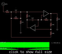
I have been experimenting with a simulation.

Going with your value for C1 and C2 as 22 nF...

To make the notch at 5 kHz...

R1 and R2 need to be 1450 ohms. (The webpage gives a slightly different result.)

I used a bipolar supply to make things easy.

Screenshot (Falstad's simulator). The scope trace shows an AC sweep from 4 kHz to 6 kHz.


I cannot explain why your layout acted as a narrow bandpass.

- - - Updated - - -

I just recalculated.
The webpage method of calculating the resistors results in almost exactly the same values which work in my simulation.

- - - Updated - - -

I see you wanted to get 5.6 kHz.
1300 ohm resistors will do.
Thanks BradtheRad
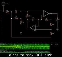
I am using TINA Circuit simulator, I am sorry about the attachment. Its about 60 Hz notch. However, I know the formula you are using to calculate value of components, but its surprising that the output is not as expected. Which simulator are you using?
 

Now I understand. You want to reduce 60 Hz.

I tried again using your component values. They work.

Screenshot is below. The notch is at 61 Hz. Scope trace is a sweep from 45 to 80 Hz.


TINA is a popular simulator, however I'm a fan of the one at:

https://www.falstad.com/circuit/

Click the link below to import my layout and run the simulation on your computer. Click Allow to make the connection.

You can adjust values at will by right-clicking on a component, to bring up an edit window.

https://tinyurl.com/9kob5dn
 

Thanks again.

Now I am an Embedded Guy who need some conceptual help with filter design. Can you tell me why did you replace Cin and Cout in my circuit with 2 resistances of 100 here?
 

I think the problem is the S11 response is very high impedance at resonance and the coupling caps are too high impedance in this frequency range, so a voltage source low impedance is required.
 

I think the problem is the S11 response is very high impedance at resonance and the coupling caps are too high impedance in this frequency range, so a voltage source low impedance is required.

I am unable to get your point. Could you elaborate a little more please.
 

Thanks again.
Now I am an Embedded Guy who need some conceptual help with filter design. Can you tell me why did you replace Cin and Cout in my circuit with 2 resistances of 100 here?

Hi,

enclosed you will find a diagram and the formulas for designing a Fliege notch filter.
Please realize the parallel connection for y1 and that some resistors must be equal.
The design is for dual supply.
Do you require single supply?
 

Attachments

  • Fliege_Notch.pdf
    301.5 KB · Views: 160

The capacitors are needed to block DC, when using a single supply with the op amp. It's because we lift its non-inverting input to supply_V /2.

Generally an op amp is easier to troubleshoot by using a bipolar supply (at least when starting out). The extra components can be omitted.

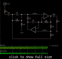
I added an input resistor to simulate some amount of impedance from the preceding stage. As it turns out, varying this resistor affects the center frequency.

I added an output resistor for a visual cue of current direction. The lower scope trace is taken across this resistor.

So the schematic seemed to work pretty well, after some experimentation.

The next step is to try the setup with a single supply.

So...

I put the 2.2 uF capacitor at input. I added a 1000 uF at output. I applied 0.9 V at V3.

I edited the op amps so they output a level between 0 and +1.8V. (Even though I'm not sure there are real op amps that can do this on a single supply of 1.8V.)

Now the simulation is no longer working as it did before. The output waveform is not a sinewave, at least not below 60 Hz.

The non-inverting inputs are seeing volt levels which wander into the negative. This causes the outputs to go to zero for a time.


Right now it's working better after I attenuated the input waveform, and raised the volt level at V3 to 2V.

It will take more tinkering to obtain normal operation, if it is possible.
 

Hello,
I am trying to design a Fliege Notch Filter at 5.6 KHz for design of neuronal signal acquisition system. I am using op-amp OPA2333 with single supply. However the output to the circuit amazed me because it acts like an narrow band pass filter instead of notch filter.
I really appreciate if someone could point out the error. Attached is the simulation Circuit and Output.
I have done this design on the basis of basic steps mentined in https://www.ti.com/lit/an/sloa093/sloa093.pdf Page 9

Hi, the circuit as shown in the TI documentation for single supply does not work (as you have noticed).
Do the following:
*Remove V3 and ground the resistor R3 instead.
*Use a high-resistive voltage divider 2:1 (two equal resistors) directly at the input of the circuit to bias this input with 0.5*Vcc.
*Use a large coupling capacitor for the input signal.

This should work. More than that, I recommend the dimensioning as shown in my former post.
Good success.
 

TINA is a popular simulator, however I'm a fan of the one at:

https://www.falstad.com/circuit/

I would suggest shavarna.jiit sticks to TINA (or maybe LTspice). That Java applet is extremely slow and that is with a simple circuit. Also, you would want to be doing an AC analysis with log scales for filter design and evaluation.

Keith
 

I would suggest shavarna.jiit sticks to TINA (or maybe LTspice). That Java applet is extremely slow and that is with a simple circuit. Also, you would want to be doing an AC analysis with log scales for filter design and evaluation.
Keith

Yes, I strongly support this recommendation.
A filter simulation in the time domain only - without the chance to see how the frequency response looks like - is really "nothing".
Neither you can identify the notch frequency (with sufficient accuracy) nor the depth of the notch as well as the quality factor (sharpness of the notch).
 

Hi, the circuit as shown in the TI documentation for single supply does not work (as you have noticed).
Do the following:
*Remove V3 and ground the resistor R3 instead.
*Use a high-resistive voltage divider 2:1 (two equal resistors) directly at the input of the circuit to bias this input with 0.5*Vcc.
*Use a large coupling capacitor for the input signal.

This should work. More than that, I recommend the dimensioning as shown in my former post.
Good success.

One possible alternative would be, of course, if the signal source (an amplifier stage?) could provide this dc level of Vcc/2.
 

Hi, the circuit as shown in the TI documentation for single supply does not work (as you have noticed).
Do the following:
*Remove V3 and ground the resistor R3 instead.
*Use a high-resistive voltage divider 2:1 (two equal resistors) directly at the input of the circuit to bias this input with 0.5*Vcc.
*Use a large coupling capacitor for the input signal.

This should work. More than that, I recommend the dimensioning as shown in my former post.
Good success.

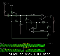
I relocated the 0.5*Vcc level as you suggested. This has greatly improved performance.

I also made the input amplitude 1/2 V. I made input and output impedance 1k ohms.

The input capacitor needs to charge for a few cycles at power-up. While it is charging the output has jagged spikes instead of a sine.

The scope trace shows about 40 to 80 Hz. Notch frequency is 59 to 61 Hz.


I relocated the 0.5*Vcc level as you suggested. This has greatly improved performance.

Yes, that's the second alternative for proper biasing in case of single supply.
For clarification, here again are all three solutions for providing the input with a bias Vcc/2:

1.) Use a separate voltage divider 2:1, which is driven by Vcc (as mentioned in post 10), or
2.) Use only one single additional resistor of 100k driven by Vcc/2 (as shown by BradtheRad in post 14), or
3.) Use the dc level Vcc/2 of the driving signal stage (if available).
 

Hi, the circuit as shown in the TI documentation for single supply does not work (as you have noticed).
Do the following:
*Remove V3 and ground the resistor R3 instead.
*Use a high-resistive voltage divider 2:1 (two equal resistors) directly at the input of the circuit to bias this input with 0.5*Vcc.
*Use a large coupling capacitor for the input signal.

This should work. More than that, I recommend the dimensioning as shown in my former post.
Good success.

Thanks a lot LvW. It worked perfectly. Could you explain the changes you made here. Please , its important for me to understand the concept.
 

Thanks a lot LvW. It worked perfectly. Could you explain the changes you made here. Please , its important for me to understand the concept.

The answer is simple:
In case the filter has to be operated with a single supply Vcc it is necessary that the opamps are biased with a quiescent voltage Vcc/2.
That means: Both opamp outputs as well as both inputs of each opamp must have this dc potential (vs ground) of Vcc/2.
Then, mark in the circuit diagram these 6 nodes carrying Vcc/2. Now - when you realize that between these nodes no dc current is allowed (in order to keep the potential Vcc/2) it follows that also the input must have the same potential Vcc/2 (because no dc current is allowed through both 2.4Mohm resistors). This voltage must be provided externally.
 

Status
Not open for further replies.

Part and Inventory Search

Welcome to EDABoard.com

Sponsor

Back
Top