Practical VNA calibration methods using Anritsu MS2024B

Status
Not open for further replies.

BusyEng

Newbie level 6
Joined
Jan 8, 2014
Messages
14
Helped
0
Reputation
0
Reaction score
0
Trophy points
1
Visit site
Activity points
133
Hi folks,

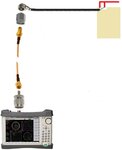
I am very new to the field of RF measurement and need some help to correctly set up the VNA, interfacing cables, connectors and DUT to make a correct measurement. Using my Anritsu MS2024B VNA, I would like to measure the impedance and Return Loss of a 2.4GHz printed antenna (such as a loop, Meander, or Inverted F antenna). These antennas are very small and are printed on very small circuit boards too. There is no room for a SMA connector to be placed on the board. Therefore, my only option is to solder a very tiny coaxial cable to the feeding points of the antenna on the PCB. I use something like Hirose U.FL-2LP-04N2-A-(200) cable that has two UFL connectors on its ends. I cut the cable on one end and come up with a cable that has a UFL connector only on one side. I solder the center wire of the free side of the cable to the feeding point of the antenna on the PCB. I also remove few millimeters of the plastic jacket to expose the shield and solder the shield to the edge of the GND plane somewhere close to the feeding point of the antenna. Then I use a UFL to SMA adapter to connect the tiny coaxial cable to a RG316 cable (such as Amphenol 135110-01-24.00). I attach a SMA to N adapter on the MS2024B to connect the other side of the RG-316 cable to the MS2024B port. The picture here shows the connections that I just explained.

My Questions here are:
1) I cannot use a regular SMA RF terminator or calibration kit here. How can I do the calibration? Can I just keep the end of the UFL cable open and consider it as Open then solder the center wire to shield and consider it as the short for calibration purpose?

2) What can I use as the 50Ω load for calibration is such application? can I just use a 50Ω 0402 SMD resistor?

3) How should l I setup the VNA for calibration? For example, How do I define the Calibration coefficients in this configuration for User-Defined Port setup? (how to find the values of Short Offset, Open Offset, Open C0, Open C1, Open C2, Open C3 variables needed for User-Defined Port Setup?)

Thanks
 

You should not connect cable to PCB such close to antenna. Measurement cable will leave PCB in a hot area and will affect ground size. This affect both radiation pattern and antenna impedance and increase problem with reflection on braid. Move point where cable leaves PCB and use ferrite-beads.
Forget UFL connector at PCB, just solder the cable as close as possible to the point for which you want to measure impedance. That place is usually the place of a matching circuit or RF pin for a radio-IC.
Each measurement object is unique how to best do calibration and measurement and it may even depend on what type of VNA that is used.

Q1. Several calibration methods are possible. I prefer to calibrate by using exact same type and length of cable as the cable that is soldered on PCB, but fitted with SMA connectors in both ends and do calibration for this cable. Next replace this cable with on PCB soldered cable and set port extension/electrical delay.
This way are almost all all losses in soldered cable compensated for, even if it is a very thin and lossy cable.

Q2. For example when PCB internal transmission lines involved in actual measurement and these must be excluded in actual measurement can matching with SMD components be needed.

Q3. Below 2 GHz and measurement in consumer products can you most likely set all coefficient to 0 when doing incircuit calibration. It is probably not ideal but good enough in most cases.
Higher frequencies can be more tricky. Calibration results depends on factors such as how stable RF ground is at measurement point and PCB as losses in return ground current along internal transmission lines that is included in actual measurement. Sometimes is it wonted to include these losses in measurement and sometimes must they be calibrated away. For calibrating "open" in an existing trace for a impedance network can "open" be loaded with a lot of stray capacitance due to several traces with unpopulated pads, how big this problem is, depends on actual PCB design and frequency range. It is mainly for "open" this cause problem.
Simplest solution is to use shortest possible traces and cut away not needed parts of traces.

Is measuring VSWR with medium precision enough, set C-coefficients to 0, calibrate SOL and do not care about port-extension/electrical delay. VSWR will be reasonable correct but Smith-chart will show rubbish.
**broken link removed**
 
Status
Not open for further replies.
Cookies are required to use this site. You must accept them to continue using the site. Learn more…