Continue to Site

Welcome to EDAboard.com

Welcome to our site! EDAboard.com is an international Electronics Discussion Forum focused on EDA software, circuits, schematics, books, theory, papers, asic, pld, 8051, DSP, Network, RF, Analog Design, PCB, Service Manuals... and a whole lot more! To participate you need to register. Registration is free. Click here to register now.

practical implementation of feedback in layout

Status
Not open for further replies.

yefj

Advanced Member level 5
Joined
Sep 12, 2019
Messages
1,505
Helped
1
Reputation
2
Reaction score
5
Trophy points
38
Activity points
9,114
Hello i have a circuit shown bellow,as you can see my feedback line crossed the Vin line.
Is there some method of routing on how to overcome this obsticle?
Thanks.
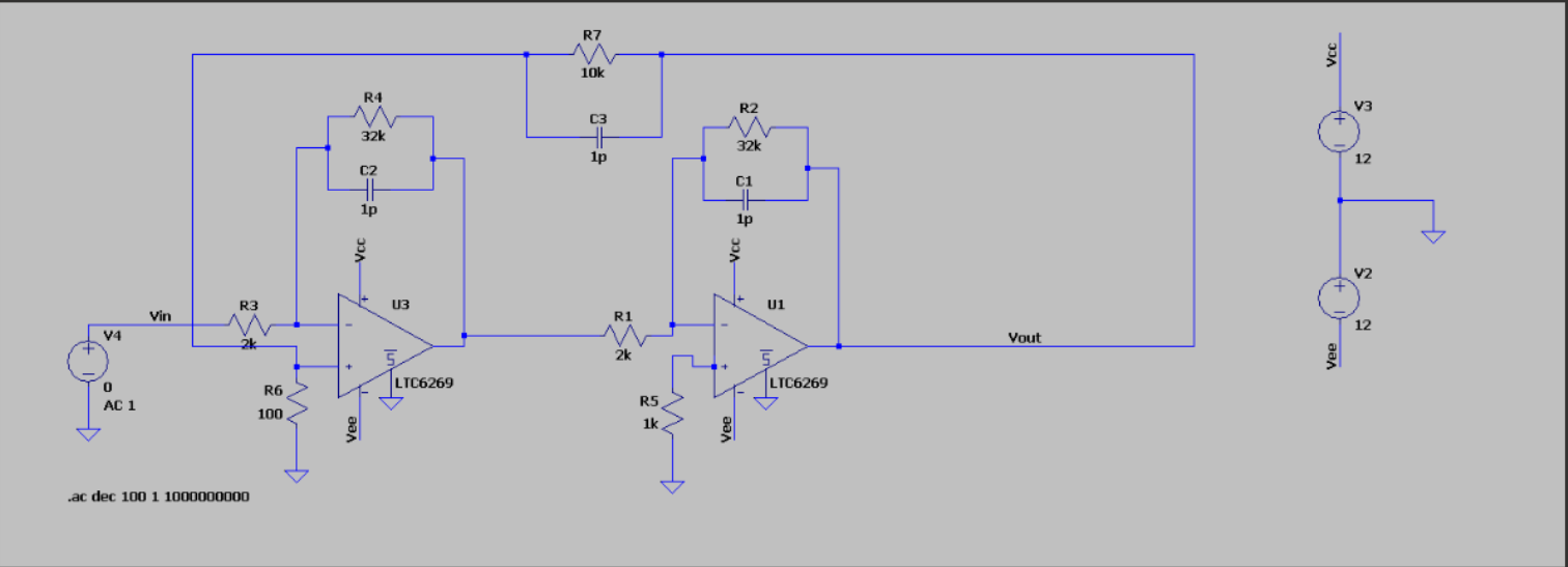
1688234373589.png
 

Hello i have a circuit shown bellow,as you can see my feedback line crossed the Vin line.
Is there some method of routing on how to overcome this obsticle?
Thanks.

View attachment 183599
why is this a problem? There’s no connection dot, so the wires aren’t connected where they cross. If it really bothers you, for some strange reason, then run the feedback circuit along the bottom
 

Hello Barry and Klauss ,basicly I want an advice regarding metal layer strategy.
My basic strategy is as shown in photos 1 and 2 where i have 4 matel layers M1 to M4.
I am using M2 and VIAS to connect the V_plus of the opamp and the output of the amplifier.
GND is metal 4 which will be connected with via to the SMD components.
M3 layer could be used for powering the opamps using VIAS from M3 to M1 smd components.
Is it ok?
Thanks.


1688540157079.png


1688540204087.png

1688540576442.png


1688540822411.png
 

Attachments

  • 1688540128893.png
    1688540128893.png
    29.7 KB · Views: 113

Hi,

first: you posted in the "IC design" section. But I gues you don´t do IC design here.

Then
* the schematic is to show the function. It has no meaning for the physical position of an IC pin.
(You may have one IC including 4 OPAMPS, while each OPAMP may be placed on a different sheet of the schematic and additionally the power supply symbol may be also placed where ever you want. But at the PCB all 4 OPAMPS are physically connected as well as electrically but also mechanically)

So for me the question is completely odd.

Klaus
 

I have no idea what you are doing here. Why would you put ground on the bottom layer? Usually, especially if you've got controlled impedances, the ground layer is under the signal layer (layer 1, I presume here) not 3 layers away.

I'm with Klaus; this whole post is bizarre.
 

A usual scheme for 4 layer PCB is one ground, one splitted supply plane, top and bottom signal layer. From this perspective, the considerations in post #4 don't make much sense.

For a "low frequency" circuit as discussed here, trace impedances don't play a role, except for low inductance ground and supply bypass. It can be best achieved with a continuous ground plane.
 

Ok thank you for the remark so M2 is my ground.
So for the feedback loop i do a VIA from M1 (Vout trace) to M3 and do a trace inside M3 and then connect back to M1(V_plus)
problem is when i a doing a trace inside M3 what ground for my trace will i use?
you said M4 is problematic to use as ground,my ground is M2.
how can i solve such problem.
Thanks.
 

UPDATE:
please correct if my logic is wrong.
I am trying to implement the circuit bellow.
as i see it there is no way to supply both DC and AC on a simple 1 substrate 2 metal layer device because the RC connected to the opamps.
So i cannot connect -Vs and +Vs on the same layer, so i will do a VIA to M3 and draw there a trance and then another VIA from M3 to M1 +VS node.
but the M3 power supply layer also needs a ground, so should i use M4 as the ground for M3 and connect M4 and M2 grounds together with a VIA.

I know that i need a 3 pin DC connector( + ,- , GND),how do i connect it my pin to the pcb?
my the M2 GND layer is closer then M3.
So i need to cut one leg of the connector so Plus minus willbe in M1 and GND will be on M2?
Thanks.

1688751519307.png

1688751543161.png

1688751559393.png
 

Hello, so M2 will be GND both for M3 power traces and M1 AC traces.
regarding my power layer in M3 ,is it too over complicated?
as i see it there is no way to route both power and AC on the opamp as shown below,because RC traces block access to VS+
Correct?

1688753836750.png

1688753858710.png
 

Status
Not open for further replies.

Part and Inventory Search

Welcome to EDABoard.com

Sponsor

Back
Top