themaccabee
Full Member level 4
Hi,
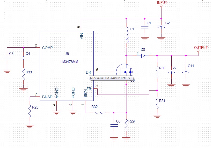
I'm trying to design a power supply of 28Vinput to 85V,200mA output.The part being used is LM3478.
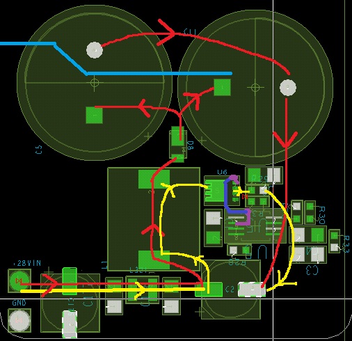
Im trying to do the layout of the same.The datasheet mentions two current loops when the the FET is ON and when the FET is OFF , these two loops should be as small as possible.
In my layout i ve tried to place all the components in a single layer..and to place the loops as close as possible..
the two loops are indicated as RED & YELLOW traces..
It is a 4 layer PCB
The bottom layer is a ground plane.
Two make the return current from C5 to flow in the same path of C11 a bottom GND plane removal is done as BLUE trace.
Also the gate drive i cant give it in the top plane since it is difficult to route between the MOSFET drain pad & Source & gate pins .I gave it using via (32mil drill dia) through an inner layer..(VIOLET TRACE) Also is there any advantage in giving it via bottom layer instead of inner layer??
I d like to know if there could be any potential problem in this layout.. particularly about the gate drive ..
Thanks for any help
Regards,

I'm trying to design a power supply of 28Vinput to 85V,200mA output.The part being used is LM3478.
Im trying to do the layout of the same.The datasheet mentions two current loops when the the FET is ON and when the FET is OFF , these two loops should be as small as possible.
In my layout i ve tried to place all the components in a single layer..and to place the loops as close as possible..
the two loops are indicated as RED & YELLOW traces..
It is a 4 layer PCB
The bottom layer is a ground plane.
Two make the return current from C5 to flow in the same path of C11 a bottom GND plane removal is done as BLUE trace.
Also the gate drive i cant give it in the top plane since it is difficult to route between the MOSFET drain pad & Source & gate pins .I gave it using via (32mil drill dia) through an inner layer..(VIOLET TRACE) Also is there any advantage in giving it via bottom layer instead of inner layer??
I d like to know if there could be any potential problem in this layout.. particularly about the gate drive ..
Thanks for any help
Regards,