Continue to Site

Welcome to EDAboard.com

Welcome to our site! EDAboard.com is an international Electronics Discussion Forum focused on EDA software, circuits, schematics, books, theory, papers, asic, pld, 8051, DSP, Network, RF, Analog Design, PCB, Service Manuals... and a whole lot more! To participate you need to register. Registration is free. Click here to register now.

Post Layout simulation at different temperature

Status
Not open for further replies.

Junus2012

Advanced Member level 5
Joined
Jan 9, 2012
Messages
1,552
Helped
47
Reputation
98
Reaction score
53
Trophy points
1,328
Location
Italy
Activity points
15,235
Hello,

I am using the Assura package with the Cadence Virtuoso,

When I do the layout extraction from Quantos, I see that it will be performed at specific temperature, by default is at room temperature (25 °C) as you can see from the image below.

However, I want to do the post-layout simulation by sweeping the temperature from -40 to 85 °C with step size of 0.5 °C. What I am thinking ia that the post-layout simulation, in this case, will only be valid at the temperature where it is extracted, on the other hand it is not realistic or practical to sweep the extraction for the tested range.

Please I need you explanation for this issue.
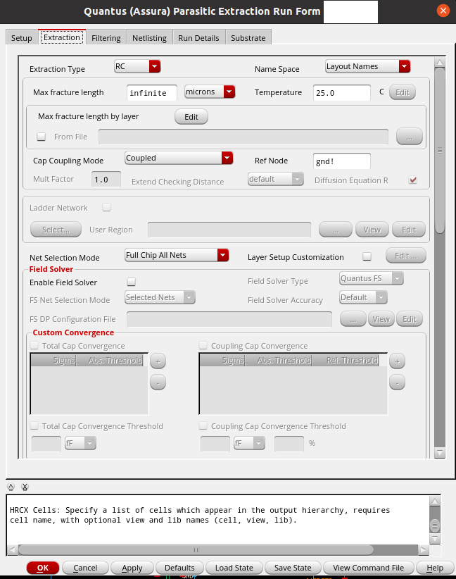
QRS.png


Thank you in advance
Regards
 

There used to be an option (at least in Calibre) to extract the parasitic with appropriate temp coefficients. In that case, depending on the simulation temperature, the parasitic value will be calculated during netlisting and this way, a single extraction would suffice. There must a similar option in Assura too.
 
Interconnect parasitics should be pretty temperature-invariant.
MOS device parasitics' temperature profiles should already have
been embedded in the model files (although the quality of that
fit is perhaps suspect, "it is what it is" unless you want to check
and maybe refine that work.

Now stepping at half degree increments sure seems like a way
to mine Bitcoin, without the Bitcoin. That is to say, gross waste
of CPU time, for what value?
 
Thank you friends for your answer
I have found the tab in Assura where I can include the temperature coefficient of the extracted resistor,
However, I agree with freebird, it will be like waste of resources to do since the active devices parasatic resistors are more dominant.

Regards
 

Hello,

I am using the Assura package with the Cadence Virtuoso,

When I do the layout extraction from Quantos, I see that it will be performed at specific temperature, by default is at room temperature (25 °C) as you can see from the image below.

However, I want to do the post-layout simulation by sweeping the temperature from -40 to 85 °C with step size of 0.5 °C. What I am thinking ia that the post-layout simulation, in this case, will only be valid at the temperature where it is extracted, on the other hand it is not realistic or practical to sweep the extraction for the tested range.

Please I need you explanation for this issue.

View attachment 175294

Thank you in advance
Regards
There is an option to save temperature coefficients in post layout netlist.

Then you can use this dspf file for any simulation / operating temperature, setting operating temperature in spice deck.
 
There is an option to save temperature coefficients in post layout netlist.

Then you can use this dspf file for any simulation / operating temperature, setting operating temperature in spice deck.

Parasitic capacitances are temperature independent, but parasitic resistances are temperature-dependent.

In advanced nodes, parasitics have a dominant effect, and their temperature dependence is important.
--- Updated ---

Crudely, variation of resistivity of common metals for interconnects - copper and aluminum - changed by ~40% over 100 deg temperature range.
For a range from -40C to 85C - 125 deg - variation is about 50%.

If 50% resistance change is not important for your designs - you can safely ignore it.
If it is important - you should take this temperature variation in account.

In almost all semiconductor companies I worked with (over a hundred), temperature dependence of parasitic resistance was included in the design flow and analysis.
 
Thank you Timof for your nice explanation that is great answer,

If I am working on 0.35 µm should I be less wary right ?

I will contact my foundry to see if they support the TC option in their PDK.
 

Thank you Timof for your nice explanation that is great answer,

If I am working on 0.35 µm should I be less wary right ?

I will contact my foundry to see if they support the TC option in their PDK.

In general, the older the technology node - the lower the importance of parasitics, and various parasitics effects (including the temperature dependence of resistivity).

However, it all depends on your design intent and requirements.
If you do power devices or PMIC in these old nodes (0.35, 0.25, 0. 18 um etc.) - you still have to care for Rdson, Rgate, low IR drop, drain dV/dt effect, guard ring resistance, etc. And if these effects are important, their temperature dependence is important as well.

There is no simple answer to a question "if parasitics are important (or not) in older technology nodes".
The answer is - "it depends".
 
Status
Not open for further replies.

Part and Inventory Search

Welcome to EDABoard.com

Sponsor

Back
Top