Continue to Site

Welcome to EDAboard.com

Welcome to our site! EDAboard.com is an international Electronics Discussion Forum focused on EDA software, circuits, schematics, books, theory, papers, asic, pld, 8051, DSP, Network, RF, Analog Design, PCB, Service Manuals... and a whole lot more! To participate you need to register. Registration is free. Click here to register now.

pos edge dff with asynchronous active low set

Status
Not open for further replies.

sharankumargoud

Newbie level 6
Newbie level 6
Joined
Jan 30, 2013
Messages
11
Helped
0
Reputation
0
Reaction score
0
Trophy points
1,281
Activity points
1,340
HI all

Can u guys please help me about the working and schematic of the pos edge async dff with active low set.
I am bit confused . Thanks in advanced
 

refer to this for hints
https://www.edaboard.com/threads/277238/

- - - Updated - - -

pos edge to neg edge is as simple as taking away or adding an inverter. active low reset vs active reset is also as simple as an inverter.
the reset or in your case set is a bit little bit more circuitry, async means its signal isnt clocked in, and so you would run it directly into the latches with the latches having a set bit (can be found in most digital books).
-Pb
 
Thank u prestone, its helped me for some extend , but i wanna reduce my circuit only nand gates, i found bit confusion where to put the active low set in the circuit.
Could you please help me out?
 

Thank u prestone, its helped me for some extend , but i wanna reduce my circuit only nand gates, i found bit confusion where to put the active low set in the circuit.
Could you please help me out?

It is better to go with Transmission gate usage ,because you can lower the transistor usage.

Post your schematic and let us know what the problem is and how to optimize it.

- - - Updated - - -


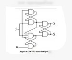
Here I have attached a schematic of positive edged D-FF with async Preset. This is with 26 Transistors.
 
dff.jpg

This is pos edge DFF , based on this i attached the asyn active low set, to the top most nand gate i.e. which r vertically placed and to nand gate with Q as output.
Hope you can understand my description. Thanks in advance
 

Sharan,

So, you want to include Aysnc Set in this architecture.

If you're student , then it is fine to go with this. But this is not a optimum schematic. NAND gate has more logical effort than Inverter. So, it is preferable to use Inverter .

So, when Set=0, The result should be Q=1 and Qbar=0.

Now, tell how you making this with this circuit. Please write it down and attach here. It will be better for understanding for other folks also.

Based on your description given, I am confused that whether the input is given to one NAND gate?. Can you please clearly mention the changes you want to do.
 

Yes, I am designing the standard cell , so to characterize its is more simple and delays will be less in nand compare to transmission gates.
I am giving set input to 2 nand gates,
one NAND which has Q as output
other one is First nand gate in top most latch .
 

Status
Not open for further replies.

Part and Inventory Search

Welcome to EDABoard.com

Sponsor

Back
Top