Continue to Site

Welcome to EDAboard.com

Welcome to our site! EDAboard.com is an international Electronics Discussion Forum focused on EDA software, circuits, schematics, books, theory, papers, asic, pld, 8051, DSP, Network, RF, Analog Design, PCB, Service Manuals... and a whole lot more! To participate you need to register. Registration is free. Click here to register now.

Port refinement, process hf3d error: Port 2 does not have a solved inside material on either side (HFSS)

An_RF_Newbie

Member level 4
Member level 4
Joined
Sep 1, 2020
Messages
70
Helped
0
Reputation
0
Reaction score
0
Trophy points
6
Activity points
572
Hi,
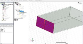
I am a newbie to HFSS, however, I have some experience with CST software. Today, I started to simulate a hollow rectangular waveguide. I placed two rectangular planes as ports on both sides of the waveguide but the HFSS showed me the "Port refinement, process hf3d error: Port 2 does not have a solved inside material on either side" error.

1)Is it necessary in HFSS to place the rectangular sheet at the end? I made the sheets longer to touch the metal, and the simulation finished but the are no acceptable port results.
2) why did this error come up? and How to solve it.
3)How is it possible to make the HFSS not consider all environments as PEC in some planes?
 

Attachments

  • Project4.zip
    26.3 KB · Views: 88
I appreciate your comment. I have uploaded the image.
 

Attachments

  • 55.JPG
    55.JPG
    189.1 KB · Views: 203
Ok, so it appears you are using a wave port. However, it appears that you do not have any metal or conducting boundary conditions in your setup. Assign a metal material to the waveguide (right now, "box2" is assigned as a vacuum), and let us know how this changes things for you.
 
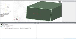
I appreciate your comment, It was my big mistake:) but it shows me another error:

[error] At least one material assignment should have solve inside set! (06:22:02 PM May 24, 2024)
[error] Simulation completed with execution error on server: Local Machine. (06:22:02 PM May 24, 2024)

It means no hollow waveguide can be simulated?
 

Attachments

  • 56.JPG
    56.JPG
    127.4 KB · Views: 137
Thank you for your collaboration, yes, it works fine, but my meaning is that we are not able to simulate it without a vacuum dielectric inside of a hollow waveguide.
 
Thank you for your collaboration, yes, it works fine, but my meaning is that we are not able to simulate it without a vacuum dielectric inside of a hollow waveguide.
If the waveguide is "hollow", there is something inside of it that is not metal. You simply need to tell HFSS what this is.
HFSS (similarly to most FEM solvers) does not generally assume a vacuum by default.
 
Here are the quick design steps for hollow waveguide design:

  1. Draw two identical rectangular boxes.
  2. Slightly enlarge one of the boxes along the x and y directions, and assign a conductive material (PEC is okay).
  3. Subtract the boxes (use the conductive box as the blank part and the vacuum box as the tool part). Ensure the "Clone tool object before operation" option is enabled.
  4. Press "F" to select faces and assign wave ports to the selected faces.
  5. Analyze and simulate.
 

LaTeX Commands Quick-Menu:

Part and Inventory Search

Welcome to EDABoard.com

Sponsor

Back
Top