Continue to Site

Welcome to EDAboard.com

Welcome to our site! EDAboard.com is an international Electronics Discussion Forum focused on EDA software, circuits, schematics, books, theory, papers, asic, pld, 8051, DSP, Network, RF, Analog Design, PCB, Service Manuals... and a whole lot more! To participate you need to register. Registration is free. Click here to register now.

polygon pour on top layer beneath BGA

Status
Not open for further replies.

rayhh27

Member level 1
Member level 1
Joined
Nov 22, 2016
Messages
34
Helped
0
Reputation
0
Reaction score
0
Trophy points
6
Activity points
361
Hi,

I am intending to design PCB using BGA IC, I am wondering whether is it not good if I use polygond copper right beneath the BGA package? Why?
Thank you.

Best regards,

RH
 

Hi,

What BGA pitch is it to have that much space?

Klaus
 

Hi,

give useful informations.

Klaus
 

Hi,

so it is like this there are many vcc, vccd_pll, etc. So like GND they are near each other and I am wondering whether it is ok to connect them using polygon.
If it is not enough what kind of information should i provide.

Thank you,

RH
 

Do you mean power planes below the BGA, common practice, suppress inner layer lands but add 0.15mm overdrill if your system supports it to get the thickest web between vias.

Suggest you have a look at this...
**broken link removed**
 

The question title suggests you want to a copper pour connecting multiple adjacent BGA balls. That's surely possible.

A side effect is however that BGA pads inside a copper pour become larger than others because they are effectively solder mask defined pads. Usually that's no problem in reflow solder.

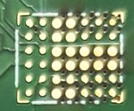
You see the effect with a BGA power IC (0.8 mm pitch) that has some pads on a copper pour:

BGA+copper pour.jpg
 

All BGA pads have nominal 0.4 mm diameter (NSMD), the isolated pads are actually etched down to about 0.35 mm. The pads inside a copper pour are effectively solder mask defined to nominal 0.5 mm, actually 0.57 mm.
 

Apart from PCB manufacturing tolerances (or possibly intentional modifications by the PCB house) visible in the example, it's exactly what you can expect when placing BGA pads on a copper pour (or traces wider than the pad).

I understood the original question so that the OP intends something similar, thus I showed this real world example to illustrate possible side effects.

In the present design, the copper pour is preferred to achieve low connection resistance for a switch mode regulator. I agree that the pad finish look curious, but I feel that it's still the best option in this case.
 

Firstly I always follow the IPC 7351 recomendation of 1:1 for solder resist openings, allowing the manufacturer to open the resist enough to get a good yield rate but avoid solder resist encroachment on pads. When solder mask defined pads come into the equation even more care is needed both from the manufacturer and the designer. If not then you can suffer bad solder joints on you BGA due to the differences in pad sizes... Round BGAs the extra added to the solder resist opening should be pretty minor to avoid exposure of copper to avoid solder shorts.
 

Status
Not open for further replies.

Part and Inventory Search

Welcome to EDABoard.com

Sponsor

Back
Top