Continue to Site

Welcome to EDAboard.com

Welcome to our site! EDAboard.com is an international Electronics Discussion Forum focused on EDA software, circuits, schematics, books, theory, papers, asic, pld, 8051, DSP, Network, RF, Analog Design, PCB, Service Manuals... and a whole lot more! To participate you need to register. Registration is free. Click here to register now.

[SOLVED] pmos bulk to drain connection error layout

Status
Not open for further replies.

preethi19

Full Member level 5
Full Member level 5
Joined
Jun 30, 2014
Messages
273
Helped
0
Reputation
0
Reaction score
1
Trophy points
16
Activity points
3,474
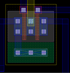
Hi i am doing layout and i read many posts saying we get soft connection error if the bulk of pmos is not given to vdd. But i need to connect the bulk to drain and this connection goes to the drain of another transistor. I am getting the "soft connection error" I couldn't make out much with what others have posted. From what i read i just understood that soft connections error occurs when connections are given through non routing layer (active and n-well). First of all can anyone please explain why does this cause a problem. Why should bulk to always to vdd and if to others an error occurs. And also can anyone please give let me know how to correct this error. Thank you!!!
 

Attachments

  • pmos.png
    pmos.png
    22.8 KB · Views: 119
Last edited:

I think you can connect drain to bulk if you connect the source to a lower potential than bulk/drain, otherwise the source-bulk diode would be biased in forward direction and inject current into the bulk.

Actually source and drain just exchange their roles, means you again have connected - former drain now is source - source to bulk, and the former source is now your drain, so should have the lowest potential.
 

Yes you are right i since source and drain are interchangeable i connected bulk to former source. But i don't think that really matters though... Does it???
Also i cant change the connection of source just so i bring it lower potential than bulk/drain... According to the ciruit i just have to give the source to vdd which i did using metal 2 ad placing a vdd pin. I am getting 3 errors in total.
2 is the soft connection error and 1 error is on gnd pin its saying"1 label/pin is on the net with a different name"... Does this have to do anything with the soft connection problem. I read that "label/pin error" occurs when there is a short circuit. But i have done the layout connections just according to the schematic. How can i find which net connection has the different name and is giving the problem... Because i saw correcting some errors corrected the others as well. Are these both related in any way???? Could anyone please help me!!!
 

Yes you are right i since source and drain are interchangeable i connected bulk to former source. But i don't think that really matters though... Does it?
Not really.

Also i cant change the connection of source just so i bring it lower potential than bulk/drain...
This would be ok.

According to the ciruit i just have to give the source to vdd which i did using metal 2 ad placing a vdd pin.
This is just what you should not do: VDD is the highest potential, so source injects current into the bulk - possibly the reason for the soft errors.

I am getting 3 errors in total.
2 is the soft connection error and 1 error is on gnd pin its saying"1 label/pin is on the net with a different name"... Does this have to do anything with the soft connection problem. I read that "label/pin error" occurs when there is a short circuit. But i have done the layout connections just according to the schematic. How can i find which net connection has the different name and is giving the problem... Because i saw correcting some errors corrected the others as well. Are these both related in any way????

I think this is an independent error. Perhaps you tried to put a pin with a name different from GND on this fixed potential node, what is not allowed.
 

Thank you so much for the reply!!! But i found the circuit in a paper and tried implementing it. I understand the concept of not giving source to high potential but if i change this connection won't it will affect the results of my circuit??? which i don't want. So i was reading about some posts of using guard rings to isolate the bulk and all but didn't quite get it fully though. But i also read pmos is already is nwell so no need for that. Guard rings are for nmos because it has the substrate floor. Without changing any connection could you please suggest a way to remove this error.

And for the label/pin error i used create pin-> typed the name gnd and gave it to the metal 2 below. Like two wide metals for power rails. Did the same for vdd and gnd. Vdd not giving any problem but gnd is. I read somewhere to include ! like gnd! I tried that too didn't work. Also for I/O type they told to select jumper for gnd and vdd. I did that too. I can't even figure out where to check regarding the gnd to correct the error.

Thank you
 
Last edited:

Please show (a minimum part of) your schematics together with the required voltage levels of S,G,D & B - and their pin names.
 

Do you think you know more about the downsides of
injecting well current, than the foundry does? This
is why, the rule. If you're going to do things that are
unproven or known bad ideas, then they want to make
sure you are forced to justify it before accepting the
mask art. Otherwise it's a bunch of boo-hoo-hoo when
the circuit latches up, and the finger points at them
and costs them engineering support hours while you try
to pin it on anything at all besides your own bad idea.

For a "test chip" you could probably get the rule violation
waived, if you provide justification and accept all of the
responsibility. For real product I would expect you'd need
to qualify this abnormal application (forward body bias)
unless the foundry has plowed that road for you. And then
there would still ought to be application rules, such as
maybe you need to put I/O-rules guard rings around any
well that is forward biased to its contents to inhibit core
latchup (where you enjoy lighter layout penalties based on
the assumption that you tied everything down in the normal
fashion, max tap spacing and all that).
 

Status
Not open for further replies.

Part and Inventory Search

Welcome to EDABoard.com

Sponsor

Back
Top