rafia123
Newbie level 3

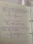
Draw the circuit diagram of a one-bit Dynamic Shift Register, based on
CMOS inverters and transmission gates, using a 2-phase,
non-overlapping clock. Briefly explain the operation of the circuit
Modify your design such that it has a parallel input and can store data
when the clock is stopped. Briefly explain its operation
For a Double Layer Metal, N-Well, CMOS technology, produce a
detailed stick diagram of the parallel load shift register cell, showing
how it connects to adjacent cells

