Continue to Site

Welcome to EDAboard.com

Welcome to our site! EDAboard.com is an international Electronics Discussion Forum focused on EDA software, circuits, schematics, books, theory, papers, asic, pld, 8051, DSP, Network, RF, Analog Design, PCB, Service Manuals... and a whole lot more! To participate you need to register. Registration is free. Click here to register now.

Place micro connector on the edges of a PCB

Status
Not open for further replies.

michcfr

Advanced Member level 4
Full Member level 1
Joined
Mar 7, 2012
Messages
106
Helped
0
Reputation
0
Reaction score
0
Trophy points
1,296
Activity points
2,011
Hello,
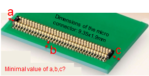
I need to place a board to board micro connector on the edges of a PCB. See the figure.
What are the minimal value of a, b, and c at the edge of the PCB?
I want to avoid mechanical problems during pluging and unplugging the connectors but when cutting the panelized PCB.
1605030978849.png


Regards,
Michel
 

HI,

I guess the connector manufacturer provides those informations.

Klaus
 

It's firstly a question of PCB design rules and secondly of panelisation techniques. For smallest distance, the PCB contour around the connector would be pre-routed with mouse bites at other places.
 

It's firstly a question of PCB design rules and secondly of panelisation techniques. For smallest distance, the PCB contour around the connector would be pre-routed with mouse bites at other places.
I agree
But what about the design rules about the minimal values at the edge of the PCB?
 

The relevant design rule is copper feature to board contour. I'd consider down to 0.5 mm as feasible. Need to check with the PCB manufacturer.
 

Status
Not open for further replies.

Part and Inventory Search

Welcome to EDABoard.com

Sponsor

Back
Top