AllenPitts
Newbie level 4

Hello EDABoard forum,
Trying to keep this simple because I think I make things to complex.

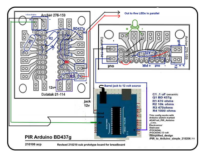
This configuration works as designed. That is when the PIR goes high output from the Arduino activates the transistor
and turns on the indicator LED on the transistor board on the left and the six more display LEDs. (The big picture is there
will be seven PIR boards and seven transistor boards that will cause the display LEDs to light according to logic on the Arduino. Presently this represents one of the PIR to LED display channels. When one channel works six more will be added.)
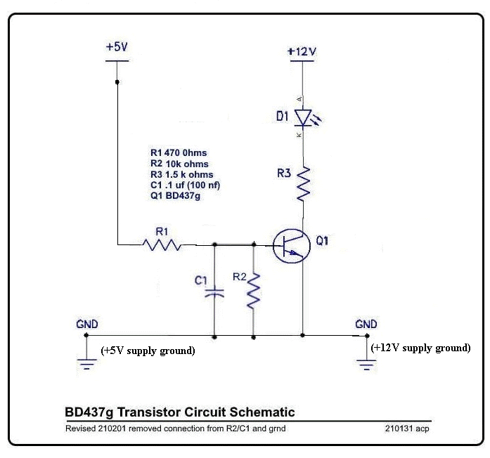
The question is about the transistor board. The transistor board is based on the excellent schematic that d123 offered recently in a thread called 'BD437g Transistor Checker'.

After I got the circuit working, the transistor to prototype board in the diagram marked PIR Arduino BD437g
the board was compared to D123's schematic to document the result. It was noticed that R2 and the capacitor (just noticed mistake on prototype diagram: the cap is shown as a polarized cap when it is really a small unpolarized cap) are connected to the BD427g base. And that R2 and the capacitor are not connected to ground as shown in the schematic.
So a jumper wire was placed on the proto board between the pads marked N1 and N2. N1 is connected to
R2 and the capacitor in parallel and N2 is connected to ground. Thus connecting R2 and C1 to ground.
When the jumper was soldered in the transistor board stopped working. And when the jumper was removed
between N1 and N2 the circuit worked again.
So without the jumper R2 and the capacitor are connected to each other but they are not connected to ground as shown in the schematic.
Question One
So why does the circuit work when it is not configured as shown in the schematic and work when it is hooked up 'incorrectly'?
Question Two
If I may be allowed a second question please: What is the function of C1 in the schematic? It is known that a capacitor stores a charge until it reaches its capacity and then releases the charge. What is C1 doing in the circuit?
Thanks for your time, knowledge and experience,
Allen Pitts, Dallas TX
Trying to keep this simple because I think I make things to complex.
This configuration works as designed. That is when the PIR goes high output from the Arduino activates the transistor
and turns on the indicator LED on the transistor board on the left and the six more display LEDs. (The big picture is there
will be seven PIR boards and seven transistor boards that will cause the display LEDs to light according to logic on the Arduino. Presently this represents one of the PIR to LED display channels. When one channel works six more will be added.)
The question is about the transistor board. The transistor board is based on the excellent schematic that d123 offered recently in a thread called 'BD437g Transistor Checker'.
After I got the circuit working, the transistor to prototype board in the diagram marked PIR Arduino BD437g
the board was compared to D123's schematic to document the result. It was noticed that R2 and the capacitor (just noticed mistake on prototype diagram: the cap is shown as a polarized cap when it is really a small unpolarized cap) are connected to the BD427g base. And that R2 and the capacitor are not connected to ground as shown in the schematic.
So a jumper wire was placed on the proto board between the pads marked N1 and N2. N1 is connected to
R2 and the capacitor in parallel and N2 is connected to ground. Thus connecting R2 and C1 to ground.
When the jumper was soldered in the transistor board stopped working. And when the jumper was removed
between N1 and N2 the circuit worked again.
So without the jumper R2 and the capacitor are connected to each other but they are not connected to ground as shown in the schematic.
Question One
So why does the circuit work when it is not configured as shown in the schematic and work when it is hooked up 'incorrectly'?
Question Two
If I may be allowed a second question please: What is the function of C1 in the schematic? It is known that a capacitor stores a charge until it reaches its capacity and then releases the charge. What is C1 doing in the circuit?
Thanks for your time, knowledge and experience,
Allen Pitts, Dallas TX
Last edited:
