Continue to Site

Welcome to EDAboard.com

Welcome to our site! EDAboard.com is an international Electronics Discussion Forum focused on EDA software, circuits, schematics, books, theory, papers, asic, pld, 8051, DSP, Network, RF, Analog Design, PCB, Service Manuals... and a whole lot more! To participate you need to register. Registration is free. Click here to register now.

pin map error after pex analyse in calibre

Status
Not open for further replies.

marziye

Newbie
Newbie level 1
Joined
May 10, 2022
Messages
1
Helped
0
Reputation
0
Reaction score
0
Trophy points
1
Activity points
19
hi

I'm using 6.1.7 cadence and I completed the layout of my design.

I have done DRC and lvs analyze without error but when I want to do pex analyze, after I did the calibre view setup I got this message that I don't know what should I do.


I'm using 65nm technology.


I'm looking forward to helping.
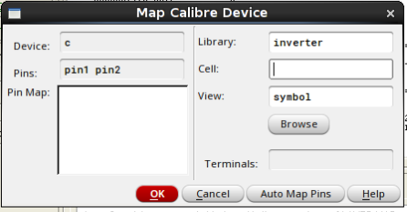
Capture1.PNG
 

Hi there,

My guess would be, you need a cell-mapping file used by PEX for "calibre" view generation.
It should be in your PDK directory under Calibre rule-decks... try to search for "calview.cellmap" file. That's how it is called in my case...

Shlooky
 
Last edited:

Status
Not open for further replies.

Part and Inventory Search

Welcome to EDABoard.com

Sponsor

Back
Top