Continue to Site

Welcome to EDAboard.com

Welcome to our site! EDAboard.com is an international Electronics Discussion Forum focused on EDA software, circuits, schematics, books, theory, papers, asic, pld, 8051, DSP, Network, RF, Analog Design, PCB, Service Manuals... and a whole lot more! To participate you need to register. Registration is free. Click here to register now.

[PIC] PIC18F66J60 pinout confusion

Status
Not open for further replies.

K33rg4t3

Full Member level 3
Full Member level 3
Joined
Aug 2, 2015
Messages
165
Helped
7
Reputation
14
Reaction score
7
Trophy points
1,298
Visit site
Activity points
2,607
Hey,
I have another question, because this is extremaly confusing.
When you look at the DOT of pinout schematic of the PIC18F66J60 datasheet, you can see that dot is in the UPPER LEFT CORNER of the chip.
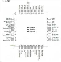
but when you look at the real life photo of the PIC18F66J60, you can see that the dot is in the LOWER LEFT CORNER of the chip.
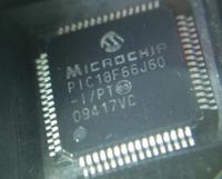
and I don't know how am I supposed to solder it. Which pin is first??
 

Starting from the corner closest to the DOT or circular impress in a counterclockwise direction, pin 1 is the first pin you will encounter. Simply rotate the package so that the DOT or circular impression is aligned with that indicated on the pinout diagram, the position of the stenciling is irrelevant.


BigDog
 

Really? Well, so that explains why the first chip was getting so hot when I connected it... you know, the "datasheet's way".
 

The pin Number one is ofcourse near the circle. There is no double thought on this. The IC getting heat is may be because there could be some mistake in the hardware connection. Try to find out that if not post the circuit we will try to do it.

Before that check the VCC and ground pins in the complete IC. Make sure all the VCC and ground pins connected correctly without any mistake and check for the input voltage level also.
 

Status
Not open for further replies.

Similar threads

Part and Inventory Search

Welcome to EDABoard.com

Sponsor

Back
Top